1. 引言
随着微电子技术和产业的发展,小型化和集成化成为微电子器件的特征 [1] [2] 。于是高介电常数材料在微电子器件中,特别是在动态随机存储器(DRAM)中有着广泛的应用前景。高介电常数材料一般具有大于1000的介电常数,近年来,人们找到了几种具有高介电常数的材料,如掺杂有钙钛矿的BaTiO3 [3] [4] [5] ,它有高于5000的介电常数,但是这么高的介电常数只能在其很窄的相变温度附近才可以得到;CaCu3Ti4O12(CCTO) [6] [7] [8] 被研究的比较多,它的介电常数高于10,000,主要来源于其本身的晶界效应(IBLC)和电极接触效应,但其有比较高的介电损耗;Li-doped NiO [9] 也有高于10,000的介电常数,但是也具有比较高的损耗。最近,一种新的高介电常数低介电损耗陶瓷材料被Hu [10] 等人发现,金红石TiO2(R)共掺杂有In2O3与Nb2O5时,具有10,000以上的介电常数的同时具有5%左右的损耗,并且具有很好的频率(100 Hz~1 MHz)、温度(25 K~450 K)稳定性,此研究非常有利于DRAM的发展与应用。作者提出的电子钉扎缺陷偶极子效应理论,合理地解释了Ti1-2xInxNbxO2陶瓷的优异介电性能机制。Li [11] 等人通过对(In2O3 + Nb2O5)共掺TiO2陶瓷的I-V曲线研究发现,陶瓷由导电的晶粒与绝缘的晶界共同组成,晶界电容效应也在Ti1-2xInxNbxO2巨介电陶瓷中起着重要的作用。Ti1-2xInxNbxO2巨介电材料的出现,有望解决传统高介电材料的许多缺点,如稳定性差、损耗高等问题,因此在高储能电容器、高密度存储设备等领域显现出极大的应用优势。基于Al2O3相较于In2O3比较便宜,并且都处于第三主族,离子半径与Ti4+很相近,因此我们用Al2O3和Nb2O5共掺杂于锐钛矿TiO2(A)中,探索制备工艺,通过一系列仪器(X射线衍射仪,扫描电子显微镜,拉曼光谱仪,HP4294A阻抗分析仪,HP4284LCR电桥和美国JANIS低温制冷系统等)的测试研究其是否也具有优异的介电性能,并探究其机制。
2. 实验方法
本实验采用传统固相烧结法制备Ti1-2xAlxNbxO2陶瓷。主要步骤有:配料–混合球磨–预烧–成型–烧结 [12] 等5个环节,具体方法如下:
1) 配料
配料是将需要原料按一定比例称量的过程。配方确定后,必须按配方称量各种原料和进行必要计算。按照计算结果,便可进行称料。本工作中,Mettler Toledo公司生产的PB230-N型电子称作为原料的称量仪器,称量精确度为0.001克。将高纯度的锐钛矿TiO2(A相99.8%)、Al2O3(99.99%)与Nb2O5(99.99%)粉末按化学计量计算后称量配料。分别配置x = 0.5%、1%、2%与5%摩尔质量的Ti1-2xAlxNbxO2粉末。
2) 混合球磨
混合球磨的机械有:球磨机、气流机、砂磨机和粉碎机等,球磨机和砂磨机是使用最多的。在本实验中,球磨机完成原料的混合。为了减少杂质的混入,我们采用尼龙球磨罐、玛瑙球。将适量的无水乙醇加入到称量原料中,然后在球磨机上球磨24小时。最后,将球磨好的原料、无水乙醇倒入烧杯,放进烘箱使其烘干,温度设定为80度,保温8小时,取出烘箱中的烧杯,把烘干的粉料取出待用。
3) 预烧
预烧的过程是化学合成过程。进行预烧有三个目的:第一,除去挥发性杂质和水分;第二,可以降低烧结时候体积的缩小;第三,使氧化物反应形成所需要的固溶体。从理论上说,较高的温度是有益的,因为它会使原料更充分的反应,但如果温度太高,它会使粉料太硬,难以研磨。所以,选取的预烧温度要适中。本实验中,我们将经球磨后烘干的原料放在烧结炉中在1100度的温度下预烧4个小时。
4) 成型
成型是将造粒好的粉末倒入模具,在直接压力的作用下形成一定的形状的方法。成型前首先需要造粒,将一定量的粘合剂(如浓度为7%的聚乙烯醇水溶液)加入陶瓷原料细粉中,制作成较粗粒度(约60目左右)、含一定水分、具有良好流动性的团粒,便于陶瓷坯料的压制成型。陶瓷粉料的大小,应尽可能小,但太细不利于成型。因为粉粒越细,就越易团聚,流动性越差,成型时填充模型不均匀,空洞易形成,导致致密度不高的坯体。成形坯体和烧结体的质量受造粒过程的影响很大,因此成形过程的关键是造粒过程。本实验中采用的单向加压成型法。为保证坯体质量,需要控制好成形压力、保压时间与加压速度等工艺参数。本实验中我们是在40 MPa的压力下干压成20 mm的圆片,保压时间为10 min。
5) 烧结
将圆片坯体加热至略低于反应熔化温度并保温一段时间,再自然冷却至室温热处理的工艺称之为烧结。样品放在高温烧结炉中,在空气气氛下烧结。烧结过程有升温、保温和降温等几个阶段,其中有两个重要参数:烧结温度和保温时间。烧结温度和烧结时间对烧结陶瓷的性能有很大的影响。本实验中,我们将圆片在1500度下焙烧10个小时,即可得到我们需要的陶瓷样品。
3. 结果分析
从图1可以看出,所有样品均为多晶结构,并且都有很好的结晶度。TiO2烧结前所有的晶相均为锐钛矿相(A相),与典型的四方结构TiO2(A)PDF卡(PDF: 21-1272)相匹配。在1500度烧结后,即使掺杂5%的高掺杂样品,也由锐钛矿相(A相)转变为纯净的金红石相(R相),四方结构TiO2(R)与PDF卡(PDF: 21-1276)相匹配。所有的样品中均没有发现其它的二次项多晶物或杂相(Al2O3、Nb2O5相等),由此可见低于5%的Al、Nb掺杂量对于我们的陶瓷的物相组成基本没有影响。Al3+离子的半径为67.5 pm,Nb5+离子的半径为78 pm,Ti4+离子的半径为74.5 pm,所有样品中的部分Ti4+离子被Al3+和Nb5+很好的替代。
拉曼光谱也可以很好的证实陶瓷的晶体结构,金红石TiO2中有四种拉曼特征峰:分别为B1g(143 cm−1),Eg(447 cm−1),A1g(612 cm−1)和B2g(826 cm−1) [13] 。B1g(143 cm−1)拉曼峰是O-Ti-O键的变角振动峰,A1g(612 cm−1)是Ti-O的伸展方式。而Eg(447 cm−1)特征峰和氧空位有关 [14] 。如图2所示,我们的样品中出现了金红石TiO2所有的拉曼特征峰 [15] ,再一次证明了用传统的固相烧结的方法合成的所有TiO2样品均是纯金红石相,这与之前我们用XRD测试的结论一致。
从图3我们可以清楚的看到,各组分的陶瓷晶粒都已经完全生长,晶界清晰可见,它们的晶粒大小均在10 um~50 um之间,晶粒大小差别不大,在所有的样品中无气孔和孔洞,说明我们的样品陶瓷有良好的致密性。
为了进一步了解Ti0.96Al0.02Nb0.02O2陶瓷的化学元素的价态以及可能存在的极化机制,我们对样品进
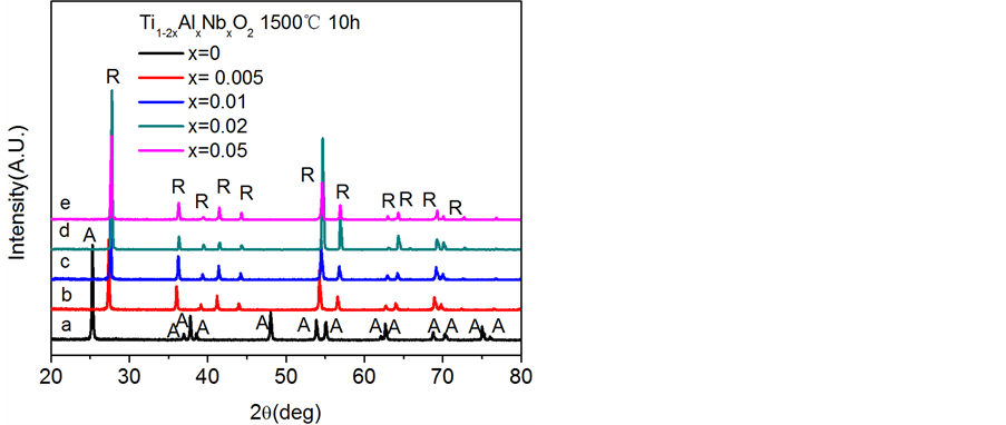
Figure 1. The XRD patterns for (a) the TiO2(A) powder and (b-e) the sintered (1500℃) Ti1-2xAlxNbxO2 (x = 0.005, 0.01, 0.02, 0.05) ceramics
图1. (a) 为TiO2(A)粉末的XRD图,(b)-(e)分别为Ti1-2xAlxNbxO2 (x = 0.005, 0.01, 0.02, 0.05) 1500度烧结后陶瓷的XRD图

Figure 2. Raman spectra of the different Ti1-2xAlxNbxO2 (x = 0.005, 0.01, 0.02, 0.05) ceramics. The dotted lines (143 cm−1, 250 cm−1, 447 cm−1, 612 cm−1 and 826 cm−1) indicate the Raman mode of rutile phase
图2. 不同浓度Ti1-2xAlxNbxO2 (x = 0.005, 0.01, 0.02, 0.05)烧结陶瓷的拉曼光谱。虚线(143 cm−1, 250 cm−1, 447 cm−1, 612 cm−1, 826 cm−1)代表代表金红石相的拉曼活性模图
行抛光后做了XPS分析测试。图4为Ti0.96Al0.02Nb0.02O2烧结陶瓷的XPS结果。Al 2p的电子束缚能是73.8 ev,如图4(a)所示,表明Al3+离子存在于样品中。人们普遍认为,Al3+作为受主杂质,取代Ti4+离子以后,晶格的电荷分布将会受到破坏,为了保持电荷平衡,需要氧空位的补偿,如以下方程:
 (3-1)
(3-1)
此外,较高的烧结温度(在此为1500度)也容易造成氧缺失,对于产生氧空位也有一定的贡献作用 [16] 。

Figure 3. SEM images for the different Ti1-2xAlxNbxO2 (x = 0.005, 0.01, 0.02, 0.05) ceramics after sintering
图3. 不同浓度Ti1-2xAlxNbxO2 (x = 0, 0.005, 0.01, 0.02, 0.05)烧结陶瓷表面的SEM图
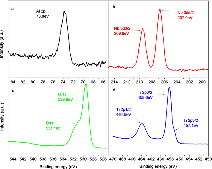
Figure 4. The valence state for the Ti0.96Al0.02Nb0.02O2 ceramic after sintering. (a) Al 2p, (b) Nb 3d, (c) O 1s, and (d) Ti 2p. The peak positions and their splitting values are also labeled in each image
图4. Ti0.96Al0.02Nb0.02O2烧结陶瓷的价态图(a) Al 2p,(b) Nb 3d,(c) O 1s和(d) Ti 2p。峰的位置以及数值在图中已经标出
图4(b)是Nb 3d电子的束缚能,3d5/2和3d3/2分别为207.0 eV和209.8 eV。自旋轨道分裂差为2.8 ev,与Nb5+单独掺杂TiO2陶瓷的分裂差相吻合 [17] [18] [19] 。由此可见,Nb以+5价态存在于我们的样品中。图4(c)为(Al + Nb)共掺TiO2陶瓷的O 1s的XPS曲线,由图可见,该峰呈现非对称结构,529.9 eV主峰位置对应于八面体金红石相TiO6的Ti-O键 [19] ,同时我们可以看到,在高能峰(531.1 eV)处还有一个很强的肩峰,因为我们的样品中不存在杂相,所以我们认为有可能是由氧空位引起的 [20] 。图4(d)为Ti 2p轨道的电子能谱,我们可以清楚的看到有3个峰,主峰Ti 2p3/2和Ti 2p 1/2的电子束缚能分别是458.6 ev和464.5 ev,Ti 2p3/2结合能与金红石TiO2(2p3/2 458.5 eV)一致,另外自旋轨道分裂差为5.9 ev与金红石TiO2(5.7 ev)相一致 [19] ,这个值有细微的差别是因为Al、Nb元素的引入。除此之外,我们还看到在低端能(457.1 eV)处还存在一个Ti 2p3/2的伴峰,因此,图4(d)的结果表明Ti离子以Ti4+与Ti3+的混合价态存在。在(Al + Nb)共掺TiO2样品中Ti4+转化为Ti3+的原因归因于引进的Nb5+破坏了原始晶格的电荷平衡或者氧空位,使Ti4+离子诱导成为Ti3+离子,方程如下:
 (3-2)
(3-2)
Nb5+代替Ti4+带一个正电荷,为了保持电荷平衡,周围的Ti4+得到一个电子变成Ti3+离子。Al3+代替Ti4+离子带一个负电荷需要相应的正电荷补充来使Ti4+去保持+4价态,为了保持电荷平衡就需要一些氧空位的存在。带正电荷的氧空位和 都可以与带负电荷的
 和
和 形成复杂的电偶极子,这些电子电偶极子缺陷是大量的,并且均匀的分布于陶瓷中,所以样品具有如此大的介电常数;额外的束缚电子被这些缺陷电偶极子簇紧紧的限制着,而不能做远距离的跳跃传导,这导致了在外部电场的作用下在很宽的频率范围内仍然保持着较低的介电损耗。
由图5(a)可知,随着温度的升高,陶瓷的介电常数也随之增大,损耗却随着减少。当烧结温度到达1500℃后,介电常数不再增大,此时,损耗也降至最低,基本维持在5%左右。介电常数增大的原因可能因为 [21] 随着温度的升高,缺陷偶极子簇与电荷增多;但这些电荷受到缺陷偶极子簇的限制不能自由移动,所以损耗才不会升高,反而降低一些。从图5(b)中可以看到,随着烧结时间的增加,介电常数也会随之增大,而损耗变化不大。当烧结时间延长到10 h时,介电常数基本不再增大。延长烧结时间会产生更多的缺陷偶极子簇和空间电荷,这可能是介电常数增加的原因 [21] 。进一步延长烧结时间,介电常数和损耗都不再有明显的变化。由图5(c)可知,在没有掺杂杂质时,介电常数是最小的,1 MHz时有354,其值略大于未烧结的纯TiO2(~120)介电值,可能是因为高温烧结(在此为1500度)会产生一定的氧空位 [16] ,使其介电常数稍微增大。当掺杂Al、Nb时,即使是掺杂很少的浓度,其介电常数也会大大的增加,同时介电损耗得到有效的抑制。例如Al、Nb各掺杂0.5%时,其介电常数达到10,000,损耗基本在5%左右,在100 KHz时介电损耗最小为3.7%。随着Al、Nb掺杂浓度的不断提高,其介电常数也会不断的增大,当掺杂的浓度达到2%时,介电常数在1MHz达到20,000以上,介电损耗基本不变,基本维持在5%上下。继续增加掺杂的浓度,我们可以清楚的看到,其介电性能基本保持不变,这有可能是因为当掺杂浓度超过2%时,Al3+、Nb5+等替代离子已经基本饱和,不再取代Ti4+离子。综上所述,在1500℃的高温下烧结10 h的Ti0.96Al0.02Nb0.02O2陶瓷为最佳样品。
由表面势垒层电容或者晶界效应引起的界面极化可以很大程度上影响介电常数,这是广为大家所接受的 [21] 。实际上,这样一种解释已经很好地解释了CCTO [6] [7] [8] 和LSNO的巨介电常数。同时,众所周知,厚度和物质的表面粗糙度也对界面极化效应做出贡献从而影响介电性能 [21] 。因此,所有用来测量介电性能的样品在测试前都用1200目砂纸抛光,使厚度为3 mm。因此,介电性能的任何差异应该是由样品的不同制备条件所决定的,而不是外部因素例如厚度、表面粗糙度等因素造成的。为了探索表面

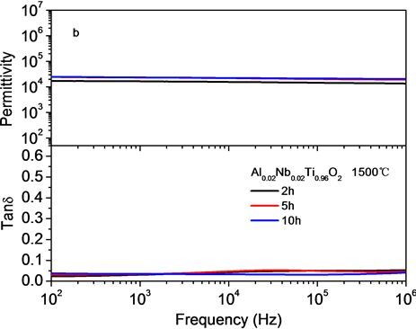

Figure 5. Dielectric properties of (a) Ti0.96Al0.02Nb0.02O2 ceramic sintered for 10 h at different temperatures (b) Ti0.96Al0.02Nb0.02O2 ceramic sintered for different sintering time at 1500˚C and (c) Ti1-2xAlxNbxO2 (x = 0, 0.005, 0.01, 0.02, 0.05) ceramics sintered for 10 h at 1500˚C
图5. (a) Ti0.96Al0.02Nb0.02O2在不同温度下烧结10 h的介电性能图,(b) Ti0.96Al0.02Nb0.02O2在1500℃下烧结不同时间陶瓷的介电性能图,(c) 不同掺杂浓度的Ti1-2xAlxNbxO2 (x = 0, 0.005, 0.01, 0.02, 0.05)在1500℃烧结10 h的陶瓷的介电性能图
势垒层电容效应在巨大介电中的影响,样品表面分别做了金电极和银电极作为测试。如图6为Ti0.96Al0.02Nb0.02O2在1500度烧结陶瓷表面涂有不同电极随频率变化的介电性能。从图中我们可以清楚的看到,当电极由Au电极变为银浆电极时,介电减少了25%左右,在100 Hz (1 MHz)从33,245 (25,552)降到25,118(19,547)。实验数据表明:当采用不同电极时,介电常数的变化可以证明表面势垒层电容效应确实存在,但是,我们观察到的介电常数的变化,与在CCTO和LSNO样品中的情况不是同一个数量级,在上述两种材料中,分别采用银电极和金电极的样品,介电常数的改变是10倍到20倍 [22] [23] 的变化。对于CCTO和LSNO,大量的移动电荷例如空间电荷、长程电子、或者弛豫极化子存在于陶瓷内,引起了表面势垒层电容效应 [24] 。在我们的Ti0.96Al0.02Nb0.02O2样品中观察到的SBLC效应尽管存在,但并不是引起陶瓷具有如此巨大介电常数的主要因素。
为了更进一步探索由晶界效应引起的界面极化的可能性,我们在直流偏压下测试了介电性能。测试

Figure 6. Frequency-dependent dielectric properties of Ti0.96Al0.02Nb0.02O2 ceramic when Ag and Au electrodes were used for the dielectric measurements
图6. Ti0.96Al0.02Nb0.02O2烧结陶瓷表面涂有不同电极(Ag和Au)时随频率变化的介电性能
的样品是Ti0.96Al0.02Nb0.02O2在1500度烧结10 h的陶瓷,电极为银浆电极。图7为在1 KHz和1 MHz时直流偏压(−10 V~+10 V)对介电性能的影响。从结果来看,在两种测试频率下介电与损耗都没有明显的随偏压而变化。在1 KHz时,当直流偏压施加时,损耗轻微的增加,但是增幅低于10%。这种增加可能来源于受限制的空间电荷。它和晶界、界面极化主宰的系统不同,那里大量的空间电荷集中在晶界,当提供一个很小的直流偏压时引起了介电和损耗的显著增加。Ti0.96Al0.02Nb0.02O2样品中,由晶界效应引起的界面极化是很微弱的。因此我们认为,Ti0.96Al0.02Nb0.02O2样品中的高介电常数的主要起源不是由晶界引起的界面极化效应所主导的。
介电温度谱,即介电常数对温度的函数关系是十分重要的实验研究,往往在介电相变或其他结构的微变化时,介电常数往往出现异常。从图8中我们可以清楚的看到,Ti0.96Al0.02Nb0.02O2样品在很宽的温度范围内(25 K~450 K)都保持稳定的高介电常数和很小的介电损耗,即介电性能很少受温度的影响,样品有很好的温度稳定性,这有利于器件的稳定。当温度低于25 K,我们可以看到,介电损耗有明显的介电弛豫,相应的介电常数减小,并随着测试频率的增加,损耗峰往高温区域移动。这与之前CCTO、Ti1-2xInxNbxO2的温度介电行为相似 [7] [10] 。我们认为有可能是当温度降到超低温区域(小于25 K)时,偶极子缺陷簇和束缚电荷被低温环境所冻结,因此引起了介电常数的减小和损耗峰的出现 [10] 。当温度高于450 K时,我们可以明显的看到高温介电驰豫,可以单单归因于Mexwell-Wagner界面极化 [10] 。在450 K以上,热激活占主导作用,引起了界面驰豫,导致介电常数和介电损耗的增大。
4. 结论
本工作中,我们通过传统的固相烧结法制备了一系列锐钛矿TiO2共掺杂的Ti1-2xAlxNbxO2(x = 0.005,0.01,0.02,0.05)陶瓷,摸索出了拥有优异介电性能的掺杂TiO2陶瓷最佳制备条件:发现当掺杂量x = 0.02时,在1500℃温度下空气气氛中烧结10 h时Ti1-2xAlxNbxO2陶瓷具有最佳的介电性能,介电常数达到20,000,介电损耗在5%左右。通过对样品的物相及晶体结构分析、微观结构、陶瓷的元素以及价态分
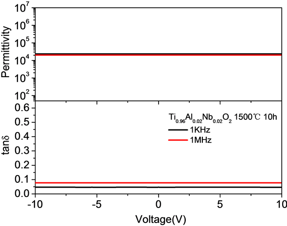
Figure 7. The relationship between the applied DC voltages (−10 V~+10 V) and the dielectric properties of Ti0.96Al0.02Nb0.02O2 ceramic measured at 1 kHz and 1 MHz, respectively
图7. 在1 KHz 和1 MHz 处Ti0.96Al0.02Nb0.02O2陶瓷的介电性能与所加直流偏压(−10 V~+10 V)之间的关系图

Figure 8. Dielectric properties of Ti0.96Al0.02Nb0.02O2 ceramic as a function of temperature (5 K to 550 K).
图8. Ti0.96Al0.02Nb0.02O2样品在不同温度下(5 K~550 K)的介电性能图
析、介电温度谱等多方面的分析,发现Ti1-2xAlxNbxO2陶瓷由锐钛矿型结构转变为金红石相结构;具有很高的致密性;陶瓷在很长的频率(100 Hz~1 MHz)范围内以及很宽的温度(25 K~450 K)范围内有很高的稳定性;表面势垒层电容效应与晶界效应引起的界面极化效应均不是引起巨介电的主要原因,优异介电性能的主要原因源于电子钉扎缺陷偶极子效应。Ti1-2xAlxNbxO2巨介电低损耗陶瓷的合成有望解决传统高介电材料的许多缺点,如稳定性差、损耗高等问题,因此在高储能电容器、高密度存储设备等领域显现出极大的应用优势,非常有利于电子技术和产业的发展。
基金项目
本论文感谢国家自然科学基金(51272166)的资助;感谢苏州大学的资助。