1. 引言
信号完整性(SI)是在高速产品中由互连线引起的所有问题,它主要研究互连线与数字信号的电压电流波形相互作用时其电气特性参数如何影响产品的性能[1] 。其实简单的理解就是只要是影响了信号质量或时序的问题,就可归结为信号完整性问题。随着信号频率的不断提高,高速互连线之间的拓扑电路的设计方法也在发生变化,当下一般对这类拓扑的设计,大都采用一些既定的方案或经验法则,往往在制板调试阶段才能发现信号的传输出现问题,这样重新再板既费时费力,又增加了成本,本文基于SI的仿真设计就是在电路设计的同时已经考虑到了SI的风险,并使用仿真工具来量化信号的各项性能指标,指定详细的SI设计规则,使设计的电路最大可能的降低风险。
国外的科技巨头早就意识到了这个问题,并拥有自己专属的信号完整性(SI)工程师,他们与电路设计师以及PCB设计师一起相互协作,共同解决在产品研发过程中所出现的信号完整性问题。根据尚普咨询给出相关数据显示,过去十年来,全球PCB持续向亚洲尤其是中国大陆迁移,中国大陆迅速成为电子产品和PCB生产大国,并且在未来几年内将继续保持快速增长,这种快速增长也必将促使国内各研究机构和公司在信号完整性理论基础、设计流程、工程实践中加大投入资金和人力。
2. 高速互联的拓扑结构
信号完整性问题并不是指某一类特定的问题,它是各种影响信号质量和时序的问题的组合叠加,又由于各种问题的相互影响,所以对某个特定的系统进行信号完整性分析往往是复杂的,比如平行走线间的反射与串扰,反射会加大串扰的程度,而串扰信号中也伴随着反射,使信号恶化更加严重。我们知道,反射的最直接原因就是互连线中阻抗的不连续,非均匀传输线,引脚、过孔、接插件,凡是阻抗发生改变的地方,信号流经时便会发生反射,造成波形失真。此外,走线分支也会造成信号路径的阻抗不连续,这使得我们在进行电路设计时需要考虑到对于拓扑结构的设计,特别是在多分支以及走线密度较大的情况下,应更多的考虑拓扑结构对于信号的影响。下面对常见的几种高速互联拓扑结构进行简要的介绍:
(1) 点对点拓扑结构
点对点拓扑结构是最简单、最常见也是最理想的连接方式,由于其单一驱动器,单一接收器的特点,整个网络的阻抗和时序关系容易控制,所以对于关键信号或对信号质量要求非常高的信号,比如高速电路的时钟信号,在条件允许的情况下尽可能的使用点对点拓扑结构。对于这种拓扑结构中的端接方式,根据需要可以选择的余地较大,既可以进行串联端接也可以进行并联端接。点对点拓扑结构
如图1(a)。
(2) T形分支拓扑结构
T形分支拓扑结构在一个芯片驱动多个负载且信号是单向传输的时候比较常用,通常使用源端串联端接方式,这种拓扑结构的关键在于T型分支的两个臂等长,如果分支不等长,各个分支处接收端信号波形将急剧恶化,所以又称为等臂分支拓扑结构。T形分支拓扑结构如图1(b)所示。
(3) 菊花链拓扑结构
菊花链拓扑结构是链式结构的一种,也是一个芯片驱动多个负载时的常用的形式,其结构的宗旨是用最短的互连传输线把所有的接收端连接起来,从主驱动器开始,通过传输线连接到与主驱动器最近的接收端上,然后查找与该接收端最近的未连接的接收端,将两者用传输线连接起来,然后再以刚加入连接的接收端为基准,再次查找最近的未连接接收端进行连接,依此类推,直至完成所有的接收端连接,连接完成后,从主驱动器开始,所有的缓冲器连接成链状。此结构的关键点是要保证主干线上第一个分支后的各个分段长度和分支桩线长度尽量短,最好小于上升时间的1/8[2] 。端接方式常使用末端并联端接,上拉、下拉、戴维南等端接都可以,但注意极少用串联端接,原因在于串联端接方式中传输线上的信号为半幅度传输,只有末端反射信号回来后才能达到满幅,所以最开始的几个分支上的接收器可能很长时间一直处于信号的中值电平附近,信号边沿出现台阶,如果有干扰噪声,很可能会造成接收器的误判。菊花链拓扑结构如图1(c)所示。
(4) Fly-by拓扑结构
该结构是菊花链拓扑结构的改进形式,区别在于分支处stub线的长度为0。由于这类链式结构的桩线长度对于各个接收端信号的质量影响很大,基本上是桩线长度越短,信号质量越好,fly-by结构由于桩线长度已经减少到了几乎为0,所以此结构比菊花链拓扑结构更容易保证信号的质量。不同于DDR2的T型分支拓扑结构,DDR3多采用fly-by拓扑结构[3] 。如图1(d)。
(5) 星形拓扑结构
星形拓扑结构是以驱动器中心,各分支从驱动端直接分开走线的一种拓扑结构,在实际应用中往往从驱动器拉出极短的一小段线再分支,这种结构如果处理得当的话可以得到较好的信号质量。端接方式采用各个分支单独进行串联端接,在串联端接电阻的选择上也分为分支等长和分支不等长两种方式。这种拓扑结构由于在驱动多个负载时,分支过多可能找不到合适的端接电阻,所以在实际使用上有一定的限制。拓扑结构如图1(e)。
3. 高速数字信号线的拓扑结构设计
在高速电路布线过程中,经常会遇到需要将走线分成2个或者多个支路的情况。如果不认真处理,将产生严重的反射,对信号的时序造成影响。
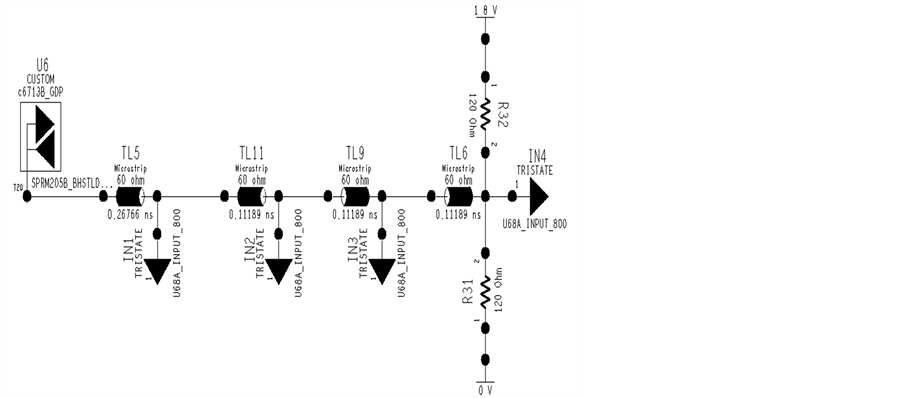
在某水声通信系统项目设计中,采用了TI公司的TMS320C6455处理器,TMS320C6455自带有一个 DDR2-533控制器,可支持最大4 Gbit的DDR2存储空间,DDR2总线数据位宽为16 bit。此外本项目使用四片Micron公司的MT47H64M16 DDR2存储颗粒组成2GbitDDR2 存储空间。由于在处理器和存储芯片间的连接存在一对多的关系,所以需要设计—个合适的拓扑结构来抑制反射。
考虑到这里对接口拓扑结构的设计属于前仿真的内容,所以先暂不考虑PCB板的层叠结构、电源网络以及目标阻抗等问题,但有一件事必须在仿真前完成,那就是给器件赋上相应的模型。从Micron公司和TI公司官网下载MT47H64M16和TMS320C6455的IBIS模型分为u68a.ibs和sprm205 b.ibs,通过Cadence的Model Integrity工具转换成.dml文件,再由Cadence仿真软件将模型导入到器件中。
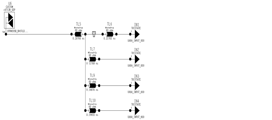
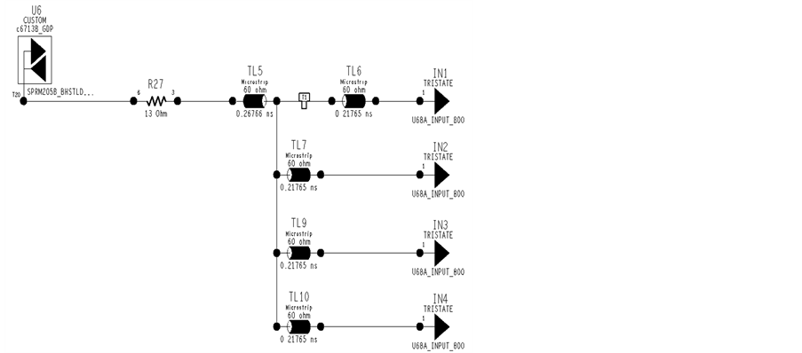
下面以TMS320C6455和各DDR2之间的某地址线为例来进行拓扑结构的仿真,其他数据线和地址线可同理对待,信号上升时间为145 ps,信号下降时间为165 ps。首先进行拓扑结构建立,这里使用理想传输线,如图2(a)。图中提取的T形拓扑结构分支并不等长且没有进行端接匹配,接收端仿真波形如图2(b)所示,图2(c)为其中一个波形的放大图,图中可以看出,接收端的波形失真严重,信号上升沿有两个非单调点,这将会造成误触发。此外对于1.8 V的信号高电平,1.970 V的最大上冲和1.635 V的最大下冲显然过大了,这将会造成近10%的信号波动,这在高速接口设计中通常是不被允许的。改进T性拓扑结构,首先利用蛇形走线使T形结构的分支等长,然后对源端进行串联端接使驱动器的阻抗与传输线的特性阻抗匹配,为了进行源端端接匹配,首先需要知道驱动器内阻,由IBIS模型中的Pullup的I/V曲线和Pulldown的I/V曲线计算得到驱动器内阻大约在43~47 ohm之间[4] ,本文选择47 ohm作为内阻,则匹配电阻为13 ohm,改进后的结构如图3(a),其接收端的波形见图3(b),图3(c)是其中一个波形的放大图,由图中所示,接收端波形大致完好,但上升沿变缓,消耗了一定的时序余量。
已知菊花链拓扑结构在一个芯片驱动多个负载时也是常用的形式,所以手动更改拓扑结构为菊花链形式,如图4(a),该拓扑中已将stub设置为0(即Fly-by结构),主干线上第一个分支后的各个分段长度尽量短并保持等距,在末端用戴维南端接匹配,用以减小反射噪声,各接收端波形如图4(b),图4(c)为其中一个波形的放大图。图中接收端波形有明显的振铃现象,并且由于戴维南端接的原因,高电平被拉低到1.257 V,低电平相应被拉高到528.9 mV,而上冲的最大幅度竟然达到1.502 V和308.9 mV,稍有噪声便难以正确接受信号。
最后进行星形拓扑结构的仿真,这是很理想的情况,即驱动端直接引出各分支,并且在各分支等长处理的情况下分别进行串联端接,串联电阻的选择满足式(1)。如果各分支不等长,那么串联电阻选择需满足式(2)。式中N为分支个数,Zout为驱动器的输出阻抗[5] 。
 (1)
(1)
 (2)
(2)
在已知驱动器内阻为47 ohm的情况下,由(1)式得Rt = −128 ohm,可知在这样的条件下无法通过串联端接的方式来使几个接受信号达到较理想的质量。星形拓扑结构如图5(a),其接收端波形如图5(b),可以看出本来比较理想的星形拓扑由于驱动器内阻过大或者负载较多,使得无法端接而令接受波形无法达到理想,此外由于此结构需要直接从驱动器引出各分支,也使得布局布线的难度加大,所以在当前这个系统中不适宜采用星形拓扑。
从以上分析中可以看出,采用菊花链拓扑结构和星形拓扑结构的接收端波形虽然整体波形未发生较大改变,但都有一定程度的失真,而采用改进后的T形结构,则使信号边沿严格单调,消除了振荡等影响,满足实际电路需求。此外,在布线完成后需要对这类关键信号再次进行仿真,即后仿真,确保设计无差错。
 (a)
(a)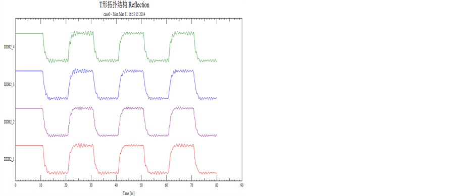 (b)
(b)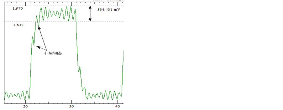 (c)
(c)
Figure 2. (a) T topology; (b) Receiving waveform; (c) Enlarged view
图2. (a) T形拓扑结构;(b) T形接收端波形;(c) 放大图
 (a)
(a)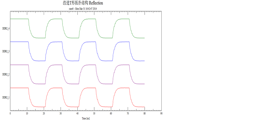 (b)
(b)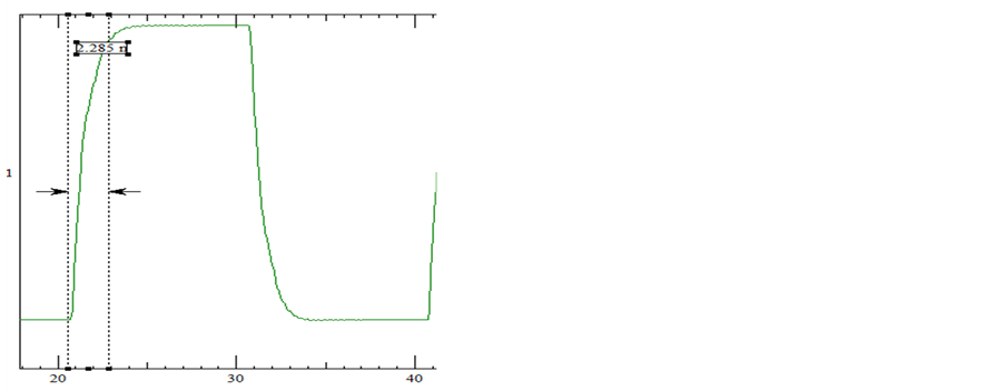 (c)
(c)
Figure 3. (a) Improved T topology; (b) Receiving waveform; (c) Enlarged view
图3. (a) 改进后T形拓扑结构;(b) 接收端波形;(c) 放大图
 (a)
(a)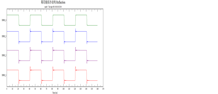 (b)
(b)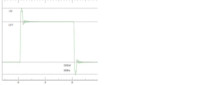 (c)
(c)
Figure 4. (a) Daisy chain topology; (b) Receiving waveform; (c) Enlarged view
图4. (a) 菊花链拓扑结构;(b) 接收端波形;(c) 放大图
 (a)
(a) (b)
(b)
Figure 5. (a) Star topology; (b) Receiving waveform
图5. (a) 星形拓扑结构;(b) 星形拓扑结构接收端波形
4. 结束语
本文分析了常见的几种高速互连拓扑结构,并且结合实际水声项目,介绍了高速数字接口电路的拓扑结构设计的一般方法,文中从对TMS320C6455和DDR2之间电路的反射仿真结果对比中可以得知,选取改进的T形拓扑结构后的信号质量明显高于其他几种拓扑结构。本文中设计的某PCB主板现已投入使用,通过对板上的DDR2存储器进行实测,所设计的高速接口拓扑结构可以在200 MHz总线速率下稳定运行,基本符合设计预期。