结电容对不同光敏元尺寸InGaAs探测器I-V特性测试的影响
Impact of Junction Capacitance on Measurement of I-V Characteristic of InGaAs Detectors with Different Photosensitive Element Sizes
DOI: 10.12677/OE.2019.91002, PDF, HTML, XML, 下载: 1,454  浏览: 3,871  国家自然科学基金支持
作者: 贺香荣, 李 淘, 徐勤飞, 杨 波:中国科学院上海技术物理研究所,传感技术国家重点实验室,上海;中国科学院上海技术物理研究所,红外成像材料与器件重点实验室,上海
关键词: 结电容效应光伏探测器InGaAs探测器I-V特性Junction Capacitance Effect Photovoltaic Detector InGaAs Detector I-V Characteristic
摘要:  I-V特性是光伏探测器最重要的表征手段之一。用电压扫描方式对光敏元尺寸为Φ 5 mm的InGaAs探测器进行I-V测试时,在负压方向电流出现了震荡现象。分析认为采样时电压处在变化中,变化的电压会引起积累在P-N结空间电荷和扩散区电荷的改变,形成P-N结电容效应而导致。本文通过测试不同光敏元尺寸探测器的零偏电阻、暗电流和电容,讨论了光敏元尺寸对InGaAs探测器I-V特性测试的影响。结果表明:随着光敏元尺寸增大,探测器的零偏电阻减小,暗电流增大,电容增大。并分析了InGaAs探测器的P-N结电容效应及其对I-V特性测试的影响,当零偏压结电容C > 10−8f @2 kHz时,I-V特性曲线在负压方向电流出现了震荡现象,测试过程中可通过限流设置或从正偏压至反偏压测试两种方式避免电流振荡现象,实现大光敏元Φ 5 mm InGaAs探测器I-V特性测试。
Abstract: I-V is one of the most important means of characterization. In voltage scanning mode of Φ 5 mm InGaAs detector for I-V test, it showed current oscillation in direction of negative pressure. It is analyzed that the change of voltage will cause accumulation of space charge and charge junction diffusion region in the P-N change, forming a P-N junction capacitance effect, resulting in the cor-responding bias dark current superimposed on a current due to charge and discharge that the capacitor brings. In this paper, the zero bias resistance, dark current and capacitance of detectors with different photosensitive sizes are tested. With the increase of the dimension size of the photosensitive element, the zero bias resistance of the detector decreases, the dark current increases, and the capacitance increases. And the P-N junction capacitance effect of InGaAs detector and its influence on I-V characteristic test are analyzed. When the zero bias junction capacitance C > 10−8f @2 kHz, InGaAs detector I-V characteristic curve produces to oscillate in the negative voltage direction. I-V test of InGaAs detector with Φ 5 mm large photosensitive element can be realized by current limiting setting or testing from positive bias to negative to avoid current oscillation.
文章引用:贺香荣, 李淘, 徐勤飞, 杨波. 结电容对不同光敏元尺寸InGaAs探测器I-V特性测试的影响[J]. 光电子, 2019, 9(1): 6-12. https://doi.org/10.12677/OE.2019.91002

1. 引言

短波红外InGaAs探测器,具有量子效率高、灵敏度高、在近室温条件下即可获得良好的性能。所以在红外系统小型化、低成本化等方面具有很强的竞争力 [1] 。InGaAs探测器研制过程离不开器件的表征,而器件的I-V特性是探测器重要的电学特性,是光伏器件最重要的表征手段之一 [2] [3] 。国内外学者对InGaAs探测器I-V特性的研究主要集中在对器件暗电流特性实验分析和理论模拟上 [4] [5] ,通过对所得I-V特性曲线的分析可以得到器件的零偏电阻和暗电流,通过对暗电流和微分电阻的拟合还可以得到材料的某些重要参数和器件工艺中引入的缺陷等信息,这些对分析和改进工艺有重要指导作用 [6] [7] 。

目前I-V测试较常采用的测试方法是电压触发,同时对电压电流值进行采样。该方法是电压扫描,采样时电压处在变化中,变化的电压会引起积累在P-N结空间电荷和扩散区电荷的改变,形成P-N结电容效应,导致在对应偏压下的暗电流上叠加一个由于电容充放电带来的电流。器件电容大,暗电流小时,就会出现振荡现象。本文就结电容对单元InGaAs光伏器件I-V特性测试的影响进行了研究。

2. 结电容对InGaAs探测器I-V特性测试影响

2.1. 结电容

PN结电容分为势垒电容和扩散电容两部分 [8] [9] 。势垒电容主要研究的是多子,是多子数量变化引起电容的变化。即当外加正向电压时,电压大小的变化,引起耗尽层宽窄的变化,及耗尽层正负电荷多少的变化,这种效应称之为“势垒电容”。势垒电容的大小与P-N结面积成正比,与耗尽区厚度成反比,反向偏置电压的增加会使耗尽区厚度增加而使势垒电容减小。正向偏置时,耗尽区厚度变小使得势垒电

容增大。势垒电容 C j = A ε s q N B 2 ( V b i V ) 。扩散电容研究的是少子,当外加正向电压变化时,引起耗尽层少子浓度及数量的变化,这种电容效应成为“扩散电容”。扩散电容 C d = A q 2 L p p n 0 k T exp ( q V k T ) 。PN

结反向偏置时电阻大,扩散电容小,主要为势垒电容。正向偏置时电阻小,主要为扩散电容。

2.2. 结电容对InGaAs探测器I-V特性测试影响

InGaAs光伏探测器的基本部分是一个P-I-N结(如图1所示),其电流电压特性(如图2所示)类似普通二极管,只是它有一个反向随光照强度变化的光电流。PN结交界处存在势垒区。结两端电压变化引起积累在此区域的电荷数量的改变,从而显现电容效应。这种电容效应的存在会影响测试结果,即在对应偏压下的暗电流上叠加一个由于电容充放电带来的电流。一般情况下,结电容充放电电流相比暗电流可以忽略,但当器件结电容较大,暗电流较小时,这种影响就变得显著起来,测试出的I-V特性曲线如图3所示。

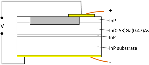
Figure 1. Schematic diagram of InGaAs detector

图1. InGaAs探测器结构示意图

Figure 2. Typical I-V characteristic curve of InGaAs detector

图2. InGaAs探测器典型I-V特性曲线

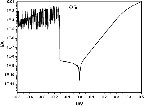
Figure 3. I-V characteristic curve of Φ 5 mm InGaAs detector

图3. Φ 5 mm InGaAs探测器I-V特性曲线

在InGaAs光伏器件I-V测试时,可以等效为结电阻( R s = V I = R s ( V ) )与结电容的并联。在交变电压下,通过P-N结的电流可分为两部分,一部分通过结电阻,一部分由结电容充放电产生。即 I s = V R s + C j V t [10] ,

其中第一项为探测器的暗电流,第二项为电容充放电电流。当暗电流较小,电容充放电电流就会产生影响,导致通过P-N结的电流变化较大,I-V特性曲线就会产生震荡现象。

3. 试验结果与改进措施

3.1. 试验结果与讨论

使用Agient B1500A半导体参数测试仪,采用电压触发同时对电压电流值进行采样,电压触发由正向负施加。测试了Φ 1 mm、Φ 3 mm、Φ 5 mm规格的InGaAs探测器I-V特性曲线如图4所示。由图4可以看出随着光敏元尺寸的增大零偏下的暗电流增大,Φ 5 mm的InGaAs探测器I-V曲线在负压方向电流出现了震荡现象,初步分析探测器的结电容太大所导致。测试了Φ 1 mm、Φ 3 mm、Φ 5 mm规格的InGaAs探测器2 kHz下的C-V特性曲线如图5所示。由图5可以看出随着光敏元尺寸的增大零偏压下探测器的结电容变大。表1给出了Φ 1 mm、Φ 3 mm、Φ 5 mm光敏尺寸InGaAs探测器的零偏电阻值、−0.1 V下的暗电流和2 kHz下零偏压下的电容值。当探测器光敏尺寸由Φ 1 mm增至Φ 5 mm时,暗电流增至原来的33倍而电容提高至原来的21倍。随着光敏尺寸的增加,暗电流和电容显著增加。

Table 1. The zero bias resistance, dark current and capacitance of Φ 1 mm、Φ 3 mm、Φ 5 mm InGaAs detectors

表1. 不同光敏尺寸下的零偏电阻、暗电流和电容

Figure 4. I-V characteristic curve of Φ 1 mm, Φ 3 mm, Φ 5 mm InGaAs detector

图4. 不同尺寸Φ 1 mm、Φ 3 mm、Φ 5 mm InGaAs探测器I-V特性曲线

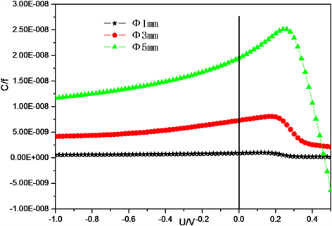
Figure 5. C-V characteristic curve of Φ 1 mm, Φ 3 mm, Φ 5 mm InGaAs detector under 2 kHz

图5. 2 kHz下不同尺寸Φ 1 mm、Φ 3 mm、Φ 5 mm InGaAs探测器C-V特性曲线

3.2. 改进措施

I-V特性曲线在负压方向电流出现了震荡现象是由于P-N结电容效应,对于自研Φ 5 mm的InGaAs探测器,材料掺杂浓度5E16,内建电场0.665 V,介电常数ε为13.9,模拟探测器的C-V曲线与实测曲线如图6所示。在负压方向实测值和模拟值基本一致。在I-V测试中有两个过程,对自然放置状态下(零偏)的探测器加电压,探测器两端电压迅速上升至设定数值,当加上反偏电压时结电容会放电,叠加在暗电流之上,显示为振荡;加正偏电压时为充电,测试正常。当结电容放电影响探测器的暗电流时,可在测试中通过设置限流来避免电流的振荡,如图7所示。当限流设置为1 mA时,I-V测试曲线正常;或测试时从正偏压至反偏压测试,加正偏电压时为充电对暗电流影响较弱,暗电流缓慢减小,I-V测试曲线正常如图8所示。

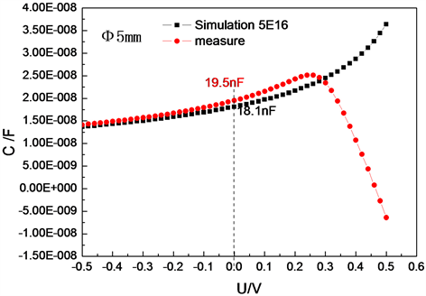
Figure 6. Capacitance simulation and measure value of Φ 5 mm InGaAs detector

图6. Φ 5 mm InGaAa探测器电容模拟值与实测值

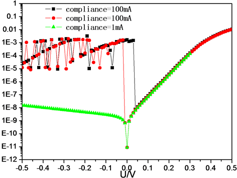
Figure 7. I-V characteristic curve of Φ 5 mm InGaAs detector at different limit current

图7. 在不同限流下Φ 5 mm InGaAs探测器I-V曲线

4. 结论

本文讨论了P-N结电容效应的存在对InGaAs探测器在电压扫描方式下的I-V测试曲线的影响,解释了当暗电流较小,电容较大时InGaAs探测器I-V测试曲线在负压方向电流出现的震荡现象。测试了不同光敏元尺寸下InGaAs探测器的零偏电阻、暗电流和电容。随着光敏元面积增大,InGaAs探测器的零偏电阻减小,暗电流增大,电容增大。并分析了InGaAs探测器的P-N结电容效应及其对I-V特性测试的影响,当InGaAs探测器的零偏压结电容C > 10−8f @2 kHz时,I-V特性曲线在负压方向电流出现震荡现象,测试过程中可通过限流设置或从正偏压至反偏压测试两种方式避免电流振荡现象,实现

Figure 8. I-V characteristic curve of Φ 5 mm InGaAs detector

图8. Φ 5 mm InGaAs探测器I-V特性曲线

大光敏元Φ 5 mm InGaAs探测器I-V特性测试。

基金项目

国家重点基础研究发展计划(973计划No. 2012CB619200)和国家自然基金(No. 61475179)。

参考文献

[1] Krabach, T.N., Staller, C., et al. (1993) InGaAs Detectors for Miniature Infrared Instruments. SPIE, 1874, 214-223.
[2] Gopal, V., Gupta, S., Bhan, R.K., et al. (2003) Isolating Surface and Bulk Contributions in an HgCdTe Junction Diode. SPIE, 5126, 215-222.
[3] Tetyorkin, V.V., Rutkowski, J., Rogalski, A., et al. (1995) Characterization of Pon-nHgCdTe Diffusion Photodioes. SPIE, 2373, 382-387.
[4] Hao, G.-Q., Zhang, Y.-G., Liu, T.-D., et al. (2004) The Dark Current Characteristics of InGaAs Pin Photodetectors. Semiconductor Optoelectronics, 25, 341-344.
[5] Forrest, S.R., Leheny, R.F., Nahory, R.E., et al. (1980) In0.53Ga0.47As Photodiodes with Dark Current Limited by Generation-Recombination and Tunneling. Applied Physics Letters, 37, 322-325.
https://doi.org/10.1063/1.91922
[6] 全知觉, 李志峰, 胡伟达, 等. 光伏型碲镉汞长波探测器暗电流特性的参数提取研究[J]. 红外与毫米波学报, 2007, 26(2): 92-96.
[7] Gopal, V., Singh, S.K. and Mehra, R.M. (2002) Analysis of Dark Current Contributions in Mercury Cadmium Telluride Junction Diodes. Infrared Physics & Technology, 43, 317-326.
https://doi.org/10.1016/S1350-4495(02)00159-7
[8] 康华光, 陈大钦. 电子技术基础(模拟部分) [M]. 北京: 高等教育出版社, 2001: 41-43.
[9] 施敏. 半导体器件物理[M]. 北京: 电子工业出版社, 1987: 53-64.
[10] Sze, S.M. (1981) Physics of Semiconductor Devices. 2nd Edition, John Wiley & Sons, Inc., Hoboken.