局域势调控下石墨烯/h-BN异质结的能带结构和量子相变
Band Structure and Quantum Phase Transition of Graphene/h-BN Heterojunction under Local Potential Control
DOI: 10.12677/CMP.2022.113007, PDF, HTML, XML, 下载: 455  浏览: 736  国家自然科学基金支持
作者: 唐婷婷, 张 军*:新疆大学物理科学与技术学院,新疆 乌鲁木齐
关键词: 石墨烯/h-BN异质结内禀自旋轨道耦合局域势量子自旋霍尔态Graphene/h-BN Heterojunction Intrinsic Spin-Orbit Coupling Local Potential Quantum Spin Hall State
摘要: 采用紧束缚方法研究了局域势调控下石墨烯/六方氮化硼异质结的能带结构及量子相变。结果表明,在给定石墨烯层内禀自旋轨道耦合强度时,石墨烯层处于量子自旋霍尔态而六方氮化硼层处于绝缘态,增大石墨烯层局域势,系统会从量子自旋霍尔态变到半导体态。调节六方氮化硼层局域势可以使异质结产生新的无间隙边缘态,从而使系统中石墨烯层的量子自旋霍尔态变成由层内和层间的边缘态共同构成的量子自旋霍尔态。
Abstract: The band structure and quantum phase transition of graphene/hexagonal boron nitride heterojunction (h-BN) under local potentials are studied by the tight-binding method. The result shows that the graphene layer is in the quantum spin Hall state and the h-BN layer is in the insulating state when the intrinsic spin-orbit coupling strength of the graphene layer is given. As the local potential of the graphene layer increases, the system will change from a quantum spin Hall state to a semiconductor state. New gapless edge states can be generated by tuning the local potential of the h-BN layer, so that the quantum spin Hall state of the graphene layer becomes the quantum spin Hall state composed of the edge states within and between layers.
文章引用:唐婷婷, 张军. 局域势调控下石墨烯/h-BN异质结的能带结构和量子相变[J]. 凝聚态物理学进展, 2022, 11(3): 57-64. https://doi.org/10.12677/CMP.2022.113007

1. 介绍

石墨烯是一种令人着迷的材料,有着较高的载流子迁移率,有希望成为新一代电子元件 [1] [2] 。但是石墨烯是零带隙,在制作元件时会导致开/关电流比很小,所以打开石墨烯带隙变得至关重要。通过在石墨烯底部施加衬底,破坏石墨烯空间反演对称性从而可以打开带隙 [3] [4] [5] 。研究人员已经通过理论计算和实验证明了六方氮化硼(h-BN)作为石墨烯衬底非常合适。h-BN是有着较大带隙的绝缘体,与石墨烯形成范德瓦尔斯异质结不仅可以破坏石墨烯空间反演对称性打开能隙,还可以保持石墨烯高迁移率等特点 [6] [7] [8] 。对于石墨烯/h-BN异质结在外场调控下的能带结构以及电子和输运已经有了广泛的研究 [9] [10] ,但是与其自旋相关的性质还了解的比较少,有待进一步深入研究。

拓扑绝缘体是一种新的拓扑状态,它的内部是绝缘状态,而边缘是导电状态,电荷只能通过边缘传播。2005年,Kane和Mele在单层石墨烯中施加内禀自旋轨道耦合(ISOC),首次预言了一种非平庸拓扑状态,量子自旋霍尔(QSH)状态 [11] [12] 。QSH状态是一种二维拓扑绝缘态,以自旋和速度方向锁定的螺旋形边缘态为特征。QSH效应受到时间反演对称性保护,其Z2拓扑不变量ν = 1。当自旋守恒时,还可以引入自旋Chern数(Cs)来表征此状态,此时Cs与Z2等价。但与Z2不变量不同的是,即使时间反演对称性被破坏,Cs依然有效 [13] [14] [15] 。在之前的工作中,我们已经知道二维电子系统考虑到ISOC时可以实现QSH效应,产生非零的量子化自旋霍尔电导,而在此基础上考虑强Rashba SOC或强无序会破坏QSH效应的稳定性,从而产生非量子化的自旋霍尔电导,形成自旋霍尔效应 [14] [16] [17] 。另外,外场的调控会使处于QSH效应或weak-QSH效应的单双层石墨烯发生拓扑相变,形成新的拓扑状态 [18] [19] [20] 。这一系列的研究都推动了自旋电子学的进步,有着重要的理论和应用价值。

基于石墨烯的这些特殊性质,研究者对石墨烯/h-BN异质结进行了大量的研究,发现了很多有趣的性质,例如次级狄拉克锥的出现,拓扑电流 [21] [22] [23] 等。但是石墨烯/h-BN纳米带(GBNNR)的许多性质仍不清楚,特别是受局域势调控下的石墨烯/h-BN异质结的能带结构和拓扑量子相变性质。在本文中,我们在晶格匹配的条件下采用紧束缚方法研究Bernal堆叠zigzag边界GBNNR在局域势调控下的能带结构及量子相变。

2. 模型与方法

单层石墨烯和单层h-BN在局域势作用下的紧束缚哈密顿量分别为:

H M L G = t 1 i , j , α C i α C j α + i λ i , j , α β υ i j C i α ( S z ) α β C j β + i , α V i C i α C i α (1)

H h - B N = t 2 i , j α C i α C j α + i , α E i C i α C i α + i , α V i C i α C i α (2)

其中 H M L B H h - B N 分别表示单层石墨烯和单层h-BN的紧束缚哈密顿量。(1)和(2)中第一项描述最近邻格点之间的跃迁,石墨烯层和h-BN层最近邻跃迁能分别为t1和t2 C i α ( C j α ) 表示自旋为 α 电子的产生(湮灭)算符;第三项中Vi表示石墨烯层和h-BN层原子在i格点的局域势。(1)中第二项为ISOC项, λ 为石墨烯层ISOC强度, i , j 表示次近邻原子跃迁 υ i j = ± 1 ,表示次近邻原子跃迁沿着逆时针(顺时针)为+1 (−1), α ( β ) = ± 是自旋指标。(2)中第二项Ei表示h-BN层B原子和N原子在i格点的在位能,分别用EB和EN表示。

Bernal堆叠石墨烯/h-BN异质结的哈密顿量为:

H = H M L B + H h - B N + t i T , j B , α ( C i α C j α + C j α C i α ) (3)

第一、二项分别为(1)和(2)中单层石墨烯和单层h-BN的哈密顿量,最后一项为层间相互作用项,B和T分别表示为h-BN层(底层)和石墨烯层(顶层)。

在研究过程中,我们通过下面公式计算Chern数 [24] [25] [26] :

C α β = 1 2 π n B Z d k x d k y ( Ω x y ) α β (4)

其中, C α β 是自旋为 α β 部分的Chern数, α ( β ) = ± 是自旋指标, Ω x y 是第n个能带在动量空间的Berry曲率 [19] [27] ,表达式如下:

Ω x y = n n 2 Im Ψ n k | v x | Ψ n k Ψ n k | v y | Ψ n k ω n ω n (5)

求和是对费米能以下所有被占据能带进行求和, v x , y = H k x , y 是速度算符。当自旋守恒时,Cs可以写成被占据空间自旋向上(C+)和自旋向下(C)之差的一半 C s = ( C + C ) / 2

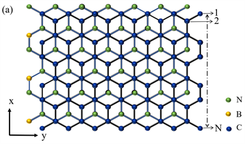
Figure 1. (a) Schematic diagram of Bernal stacking zigzag-edged GBNNR. The bottom layer is h-BN layer and the top layer is graphene layer. y is the periodic direction and the x direction contains N = 80 sites. Green, yellow and blue solid circles represent N, B and C atoms, respectively; (b) Schematic diagram of graphene/h-BN heterojunction under local potentials.V1 and V2 are applied in the upper and lower half regions of the graphene layer respectively, and V3 and V4 are applied in the upper and lower half regions of the h-BN layer respectively

图1. (a) Bernal堆叠zigzag边界GBNNR示意图。底层为h-BN层,顶层为石墨烯层。y为周期性方向,x方向包含N = 80个格点。绿色、黄色和蓝色实心圆分别表示N原子,B原子和C原子;(b) 局域势作用于石墨烯/h-BN异质结示意图。V1和V2分别被施加在石墨烯层的上半部分区域和下半部分区域,V3和V4分别被施加在h-BN层的上半部分区域和下半部分区域

3. 结果与讨论

论文研究的石墨烯/h-BN异质结是由单层石墨烯和单层h-BN通过范德瓦尔斯力结合而成。异质结的顶层为石墨烯层,底层为h-BN层,这种堆叠最稳定的构型为Bernal堆叠,即一个碳原子位于硼原子顶部,而另一个碳原子位于h-BN环中心上方如图1(a)。GBNNR中y为周期性方向,x为开边界方向包含40条锯齿链(即N = 80个格点)。局域势V1和V2分别施加在石墨烯层的上半部分和下半部分,V3和V4分别施加在h-BN层的上半部分和下半部分如图1(b)。

石墨烯和h-BN层相应的面内最近邻跃迁能分别为 t 1 = 2.64 eV t 2 = 2.79 eV ,最近邻层间跃迁能为 t = 0.43 eV ,在位能 E B = 3.34 eV E N = 1.40 eV ,如表1所示。

Table 1. Tight-binding parameters of graphene/h-BN heterojunctions calculated by density functional theory [28] (Unit of Energy: eV)

表1. 密度泛函理论计算出的石墨烯/h-BN异质结紧束缚参数 [28] (能量单位:eV)

基于以上参数我们采用紧束缚模型计算了Bernal堆叠GBNNR能带结构,如图2(a)所示。当局域势和ISOC均为零时,能带图中有一个有微小带隙,大小约为 Δ E = 20.5 meV ,这表明GBNNR是半导体。改变石墨烯层局域势V1,使其从零开始增大,发现带隙 Δ E 先增大后减小如图2(b)中红色曲线,系统始终处于半导体相。

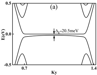
Figure 2. (a) Band structure of GBNNR with zero local potential and ISOC; (b) Band gap of GBNNR ΔE as a function of V1

图2. (a) 局域势和ISOC均为零时GBNNR能带结构;(b) GBNNR带隙ΔE随局域势V1变化图

在GBNNR中,考虑到石墨烯层ISOC (自旋轨道耦合强度 λ = 0.02 t 1 ),则系统由半导体相变为QSH相。通过改变局域势V1,可以调控GBNNR的能带结构,如图3所示。单层石墨烯中ISOC打开的体间隙为 Δ g = 2 Δ S O = 0.55 eV ,其中 Δ S O = 3 3 λ ,而在GBNNR 中,当V1=0时,由于异质结受到层间相互作用的影响,ISOC打开的体间隙实际上为 Δ g = 2 Δ S O δ ,大小约为0.49eV。图3(a)中,当费米能 | E f | < Δ g 时,系统处于QSH态,此时自旋陈数为非零值,Cs = 1。

图3(c),当 V 1 = 0.2 eV 时,系统依然具有较大的体间隙 Δ g = 0.44 eV ,局域势将体间隙中自旋向上和自旋向下的能带左右分开。费米能 | E f | < Δ g 范围内与能带有四个交点,用A,B,C,D来表示,我们计算了这四个点对应的状态概率分布如图3(d)所示,A和B表示自旋向上的状态,分别分布在石墨烯层的两个边缘处,即N = 80和1附近,C和D表示自旋向下的状态,分别分布在石墨烯层的两个边缘处,即N = 1和80附近。根据 ν y = E k k y 得到这四个边界态在纳米带中的流向示意如图3(f),A和D位于石墨烯层相同边界上,具有相反的自旋方向和传播方向,B和C与之类似,从而形成了螺旋性边缘态。这表明此时石墨烯层依然处于QSH态,自旋陈数Cs = 1。

Figure 3. Left column is the band structure of GBNNR. The red and black curves represent the spin-up and spin-down energy bands respectively. The parameters are: λ = 0.02t1, (a) V1 = 0 eV; (c) V1 = 0.2 eV; (e) V1 = 1.2 eV. (b) The blue curve is the bandgap of the heterojunction under periodic boundary conditions, i.e. the bulk gap; the red curve is the GBNNR bandgap. (d) and (f) are the schematic diagrams of the probability distributions of edge states and the edge state propagation in (c), respectively

图3. 左列为GBNNR能带图。红色和黑色曲线分别表示自旋向上和自旋向下的能带。参数为:λ = 0.02t1,(a) V1 = 0 eV;(c) V1 = 0.2 eV;(e) V1 = 1.2 eV。(b) 蓝色曲线为异质结在周期性边界条件下的带隙,即体间隙;红色曲线为GBNNR带隙。(d)和(f)分别是(c)中边缘态的波函数概率分布与流向示意图

继续增大局域势V1,体间隙 Δ g 不断减小,当 V 1 = 0.3 ~ 0.9 eV 时,体间隙与局域势几乎成线性关系: Δ g 2 Δ S O δ V 1 4 ,当 V 1 1.0 eV 时, Δ g = 0 ,如图3(b)中蓝色曲线。而当 V 1 = 0 ~ 0.5 eV 时GBNNR带隙 Δ E = 0 ,当 V 1 > 0.5 eV 时系统打开一个较小的带隙,如图3(b)中红色曲线。这说明在 V 1 = 0 ~ 0.5 eV 时,体带隙中会有无间隙的边缘态出现,此时GBNNR处于QSH相,当继续增大V1时,无间隙的边缘态消失,系统从QSH相变成半导体相,如图3(e)。

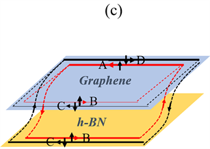
Figure 4. (a) Band structure of GBNNR with λ = 0.02 t1, V4 = −3.665 eV. The red and black curves represent the spin-up and spin-down energy bands respectively. (b) and (c) are schematic diagrams of the probability distributions of edge states and the edge state propagation in (a), respectively

图4. (a) GBNNR能带图,红色和黑色曲线分别表示自旋向上和自旋向下的能带,λ = 0.02t1,V4 = −3.665 eV。(b)和(c)分别是(a)中边缘态的波函数概率分布与流向示意图

在GBNNR的能带中,低能区域的能带主要来源于石墨烯层,h-BN层的能带则主要分布在高能区域,接下来我们通过调节局域势V4,能使h-BN层的能带向低能区域移动,从而发现了有趣的能带演化现象。如图4(a)所示,当局域势V4 = −3.665eV时,能带结构中出现了由ISOC打开的带隙,在此带隙中间有无间隙的边缘态存在。通过计算费米能Ef与能带相交的A,B,C,D四点的波函数概率分布可以知道这些态均为边缘态,如图4(b)所示。A和D分别表示自旋向上和自旋向下的状态,它们的传播方向相反,但是都分布在石墨烯层的同一个边缘处,即N=1附近。B和C分别表示自旋向上和自旋向下的状态,它们的传播方向也相反,但是它们同时分布在石墨烯层和h-BN层的同一个边缘处,即N = 80和160附近。根据边缘态的分布情况,我们可以给出边缘态在异质结中的流向图,如图4(c)所示。图中自旋向上的电流(红色虚线)和自旋向下的电流(黑色虚线)都各自形成两个闭合回路,其中一个回路在石墨烯层,另一个回路在横跨石墨烯层与h-BN层。每一个回路中,边缘态都是螺旋型的。从波函数的概率分布值上可以发现,边缘态主要分布于石墨烯层与h-BN层的两个不同边缘处,即N = 1和160处。将两个回路合在一起,系统的边缘态依然是量子化的,对应的状态为QSH态,自旋陈数Cs = 1。但是此QSH态,与单层的QSH态不同,它是由层内和层间的边缘态共同构成的。

4. 结论

本文在晶格匹配的条件下,采用紧束缚模型研究了Bernal堆叠zigzag边界GBNNR在局域势调控下的能带结构及量子相变。我们发现当石墨烯层内禀自旋轨道耦合强度给定时,石墨烯层处于量子自旋霍尔态而六方氮化硼层处于绝缘态,此时增大石墨烯层局域势强度,系统会从量子自旋霍尔相变到半导体相。而调节h-BN层局域势可以使GBNNR产生新的无间隙边缘态,从而使系统中石墨烯层的量子自旋霍尔态变成由层内和层间的边缘态共同构成的量子自旋霍尔态。

致谢

本文受到国家自然科学基金资助No. 11864039。

NOTES

*通讯作者。

参考文献

[1] Sarma, S.D., Adam, S., Hwang, E.H., et al. (2011) Electronic Transport in Two-Dimensional Graphene. Reviews of Modern Physics, 63, 407-470.
https://doi.org/10.1103/RevModPhys.83.407
[2] Rutherglen, C., Jain, D. and Burke, P. (2009) Nanotube Electronics for Radiofrequency Applications. Nature Nanotechnology, 4, 811-819.
https://doi.org/10.1038/nnano.2009.355
[3] Moon, P. and Koshino, M. (2014) Electronic Properties of Graphene/Hexagonal-Boron-Nitride Moiré Superlattice. Physical Review B, 90, Article ID: 155406.
https://doi.org/10.1103/PhysRevB.90.155406
[4] N’Diaye, A.T., Bleikamp, S., Feibelman, P.J., et al. (2006) Two-Dimensional Ir Cluster Lattice on a Graphene Moiré on Ir(111). Physical Review Letters, 97, Article ID: 215501.
https://doi.org/10.1103/PhysRevLett.97.215501
[5] Varchon, F., Feng, R., Hass, J., et al. (2007) Electronic Structure of Epitaxial Graphene Layers on SiC: Effect of the Substrate. Physical Review Letters, 99, Article ID: 126805.
https://doi.org/10.1103/PhysRevLett.99.126805
[6] Sachs, B., Wehling, T.O., Katsnelson, M.I., et al. (2011) Adhesion and Electronic Structure of Graphene on Hexagonal Boron Nitride Substrates. Physical Review B, 84, Article ID: 195414.
https://doi.org/10.1103/PhysRevB.84.195414
[7] Slotman, G.J., Wijk, M.V., Zhao, P.L., et al. (2015) Effect of Structural Relaxation on the Electronic Structure of Graphene on Hexagonal Boron Nitride. Physical Review Letters, 115, Article ID: 186801.
https://doi.org/10.1103/PhysRevLett.115.186801
[8] Fan, Y., Zhao, M., Wang, Z., et al. (2011) Tunable Electronic Structures of Graphene/Boron Nitride Heterobilayers. Applied Physics Letters, 98, Article ID: 083103.
https://doi.org/10.1063/1.3556640
[9] Sun, J., Xu, L. and Zhang, J. (2020) Electronic Structure and Transport Properties of Graphene/h-BN Controlled by Boundary Potential and Magnetic Field. Modern Physics Letters B, 34, Arti-cle ID: 2050180.
https://doi.org/10.1142/S0217984920501808
[10] Li, X., Xu, L. and Zhang, J. (2020) Band Structure and Transport Property of Graphene/h-BN Heterostructure under Local Potentials. Chinese Journal of Physics (Taipei), 65, 75-81.
https://doi.org/10.1016/j.cjph.2020.02.011
[11] Kane, C.L. and Mele, E.J. (2004) Quantum Spin Hall Effect in Graphene. Physical Review Letters, 95, Article ID: 226801.
https://doi.org/10.1103/PhysRevLett.95.226801
[12] Kane, C.L. and Mele, E.J. (2005) Z2 Topological Order and the Quantum Spin Hall Effect. Physical Review Letters, 95, Article ID: 146802.
https://doi.org/10.1103/PhysRevLett.95.146802
[13] Sheng, D.N., Weng, Z.Y., Sheng, L., et al. (2006) Quantum Spin Hall Effect and Topologically Invariant Chern Numbers. Physical Review Letters, 97, Article ID: 036808.
https://doi.org/10.1103/PhysRevLett.97.036808
[14] Sheng, L., Sheng, D.N., Ting, C.S., et al. (2005) Nondissipative Spin Hall Effect via Quantized Edge Transport. Physical Review Letters, 95, Article ID: 136602.
https://doi.org/10.1103/PhysRevLett.95.136602
[15] Prodan, E. (2009) Robustness of the Spin-Chern Number. Physical Review, 80, Article ID: 125327.
https://doi.org/10.1103/PhysRevB.80.125327
[16] Sheng, L., Sheng, D.N. and Ting, C.S. (2005) Spin-Hall Effect in Two-Dimensional Electron Systems with Rashba Spin-Orbit Coupling and Disorder. Physical Review Letters, 94, Ar-ticle ID: 016602.
https://doi.org/10.1103/PhysRevLett.94.016602
[17] Andrei Bernevig, B. and Zhang, S.-C. (2006) Quantum Spin Hall Effect. Physical Review Letters, 96, Article ID: 106802.
https://doi.org/10.1103/PhysRevLett.96.106802
[18] Xu, L., Zhou, Y. and Gong, C.D. (2013) Topological Phase Transition Induced by Spin-Orbit Coupling in Bilayer Graphene. Journal of Physics Condensed Matter, 25, Article ID: 335503.
https://doi.org/10.1088/0953-8984/25/33/335503
[19] Ren, Y., Qiao, Z. and Niu, Q. (2016) topological Phases in Two-Dimensional Materials: A Review. Reports on Progress in Physics Physical Society, 79, Article ID: 066501.
https://doi.org/10.1088/0034-4885/79/6/066501
[20] Chen, T.W., Xiao, Z.R., Chiou, D.W., et al. (2011) High Chern Number Quantum Anomalous Hall Phases in Single-Layer Graphene with Haldane Orbital Coupling. Physical Review B, 84, Article ID: 165453.
https://doi.org/10.1103/PhysRevB.84.165453
[21] Wang, E., Lu, X., Ding, S., Yao, W., Yan, M., Wan, G., et al. (2016) Gaps Induced by Inversion Symmetry Breaking and Second-Generation Dirac Cones in Graphene/Hexagonal Boron Nitride. Nature Physics, 12, 1111-1115.
https://doi.org/10.1038/nphys3856
[22] Yang, W., Chen, G., Shi, Z., Liu, C.-C., Zhang, L., Xie, G., et al. (2013) Epitaxial Growth of Single-Domain Graphene on Hexagonal Boron Nitride. Nature Materials, 12, 792-797.
https://doi.org/10.1038/nmat3695
[23] Gorbachev, R.V., Song, J.C.W., Yu, G.L., Kretinin, A.V., Withers, F., Cao, Y., et al. (2014) Detecting Topological Currents in Graphene Superlattices. Science, 346, 448-451.
https://doi.org/10.1126/science.1254966
[24] Den Nijs, M. (1984) Quantized Hall Conductance in a Two Dimen-sional Periodic Potential. Physica A: Statistical Mechanics and Its Applications, 124, 199-210.
https://doi.org/10.1016/0378-4371(84)90239-5
[25] Kohmoto, M. (1985) Topological Invariant and the Quantiza-tion of the Hall Conductance. Annals of Physics, 160, 343-354.
https://doi.org/10.1016/0003-4916(85)90148-4
[26] Hatsugai, Y. (1993) Chern Number and Edge States in the Integer Quantum Hall Effect. Physical Review Letters, 71, 3697-3700.
https://doi.org/10.1103/PhysRevLett.71.3697
[27] Chang, M.C. and Niu, Q. (1995) Berry Phase, Hyperorbits, and the Hofstadter Spectrum. Physical Review Letters, 75, 1348-1351.
https://doi.org/10.1103/PhysRevLett.75.1348
[28] Slawinska, J., Zasada, I., Kosinski, P., et al. (2010) Reversible Modifications of Linear Dispersion: Graphene between Boron Nitride Monolayers. Physical Review B: Condensed Matter, 82, Article ID: 085431.
https://doi.org/10.1103/PhysRevB.82.085431