使用十字纳米结构实现表面等离激元定向发射的超快时空控制
Ultrafast Spatiotemporal Control of Directional Launching of Surface Plasmon Polaritons Using Cross Nanostructures
DOI: 10.12677/app.2024.144018, PDF, HTML, XML, 下载: 40  浏览: 83  科研立项经费支持
作者: 邹瑷怿, 季博宇, 林景全*:长春理工大学物理学院超快与极紫外光学重点实验室,吉林 长春
关键词: 飞秒传输表面等离激元偏振控制超快时空控制Femtosecond Propagating Surface Plasmon Polarization Control Ultrafast Spatiotemporal Control
摘要: 飞秒传输表面等离激元(femtosecond propagating surface plasmon, fs-PSP)的超快时空控制是光子纳米电路元件中超快信息处理的先决条件。目前多数的研究都是集中在对SPP空间传输方向上的操控,大多集中于在空间场中实现SPP的优先发射方向的主动控制,在时间尺度实现对SPP超快调控的研究相对较少,通过使用纳米定向耦合器实现对SPP优先发射方向的超快时空调控研究几乎未见报道,在这里,利用时域有限差分(FDTD)进行仿真,研究了两种相关结构的表面等离激元的超快时空操控,解决了SPP发射方向的单一性问题,增加其超快切换方向的自由度。这项成果对优化现有的等离激元纳米电路组件中超快信息处理系统乃至拓宽其应用领域具有重要的推动作用。
Abstract: Ultrafast spatiotemporal control of femtosecond propagating surface plasmons (fs-PSPs) is a prerequisite for achieving ultrafast information processing in photonic nanocircuit components. Currently, most research focuses on manipulating the spatial direction of SPP transmission. In contrast, relatively little research has been done on actively controlling the preferred launch direction of SPPs on the time scale. The study of ultrafast spatiotemporal modulation of SPP’s preferred emission direction through nano-directional couplers has hardly been reported. Here, the ultrafast spatiotemporal manipulation of the surface plasmon of two related structures is investigated by simulation using finite-difference time-domain (FDTD) simulations, which solves the problem of the singularity of the emission direction of the SPP and increases the degree of freedom of its ultrafast switching direction. This result is an important contribution to the optimization of the existing ultrafast information processing system in plasma nanocircuit components and even to the broadening of its application areas.
文章引用:邹瑷怿, 季博宇, 林景全. 使用十字纳米结构实现表面等离激元定向发射的超快时空控制[J]. 应用物理, 2024, 14(4): 149-156. https://doi.org/10.12677/app.2024.144018

1. 引言

在与信息通信技术相关的等离子体激元领域中,表面等离激元(SPP)的优先发射方向的主动控制仍然是最具挑战性的问题之一,通过选择合适的入射光源和纳米结构,实现对光场的控制是实现SPP定向激发的可靠手段,过去已经提出了很多能实现定向激发的纳米结构,比如:单沟槽结构 [1] ,不对称圆环结构 [2] 、悬链线结构 [3] 、介电纳米天线 [4] 、V形结构 [5] 以及银圆盘阵列 [6] 等;空间中控制等离激元定向激发的手段大多是改变入射光波长 [7] [8] 、偏振 [9] [10] [11] [12] [13] 、入射角 [14] [15] 、或调节结构规格 [16] 、方位角或排列方式 [17] 等。文章中我们选择十字结构和复合十字纳米结构 [18] ,这种结构的优点是,在不同的偏振下两个狭缝对产生的SPP干涉,每个狭缝对都能在同一个方向上激发等离激元,在空间中仅通过改变偏振就能够实现激发。

表面等离激元的时空操控是制造紧凑型光学器件、控制光传播的有效手段,随着超高速数据处理 [19] 和传输的重要性日益增加,可以预见,SPP定向发射的超快时空控制至关重要,过去的研究大多集中于在空间场中实现SPP的优先发射方向的主动控制,缺乏通过使用定向纳米耦合器在纳米飞秒尺度上实现对SPP优先发射方向的超快时空控制的研究 [20] [21] ,在我们的研究中,通过选择一种复合纳米结构,目前该结构已被实验验证在空间层面可以通过改变入射光偏振态来实现SPP定向激发,在此基础上我们通过调节两束入射光0˚ (p)偏振和90˚ (s)偏振脉冲的入射方式,在时空中实现其超快操纵,这有利于等离激元纳米电路的发展,有利于加快电子器件小型化的实现。

2. 模拟参数设置

结构设置为多个狭缝对垂直排列的几何形状,使用Lumerical FDTD solutions软件进行数值模拟,将两个正交排列的凹槽刻蚀在200 nm厚的金膜上,金的介电常数取自Johnson 和Christy [22] 的实验数据。十字结构的凹槽尺寸L = 460 nm,w = 40 nm;复合结构的凹槽尺寸L1 = 460 nm、L2 = 400 nm、d = 410 nm、w = 40 nm;基底是二氧化硅(SiO2)厚度300 nm,周围介质为真空,折射率为1,监视器位置放在AU膜上方5 nm处,模拟时采用全场散射场光源(TFSF),同时采用光源垂直入射的方式,入射光选择为具有两个相对时间延时的激光脉冲,模拟中使用的入射光参数为:两束正交偏振的入射光,使用的中心波长由计算凹槽共振峰决定,相对延时时间可以用模拟软件调整,我们选择相对时间延时为200 fs;适当的边界条件是模拟的基础,在FDTD模拟中,我们采用完美匹配层(PML)作为边界条件。

3. 结果与讨论

3.1. 双光束入射激发纳米十字结构

我们首先选择十字结构进行模拟,如图1(a)为时空操控fs-PSP定向激发的原理图,其中,S1位置和S3位置分别代表+X和−X方向;S2和S4分别代表+Y方向和−Y方向;0˚线偏振和90˚线偏振光从结构下方入射,通过仿真计算该尺寸凹槽共振峰对应的中心波长,从而选择两束光的中心波长为1645 nm,相对时间延时200 fs,图1(b)为该结构的平面图,两个凹槽完全相同L = 460 nm;相对时间延时200 fs。

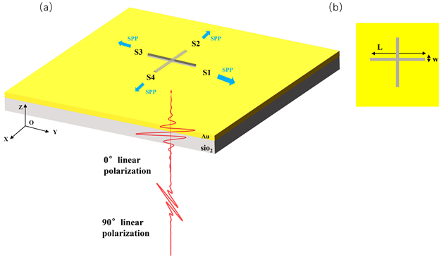
Figure 1. Spatio-temporal control fs-PSP directional excitation schematic diagram

图1. 时空操控fs-PSP定向激发原理图

图2(a)为0˚和90˚两束偏振光在延时为200 fs时叠加后的脉冲时间信号;图2(b)为S1和S2位置处的时间监视器结果,激光脉冲发射SPP的过程可分为两部分:(i) 在280 fs之前,由0˚偏振光的前半部分激发,此时与Y轴平行的凹槽发挥作用,SPP在S1和S3位置处激发;(ii) 在280 fs~480 fs,由0˚偏振光的后半部分和90˚偏振光的前半部分叠加产生的瞬时偏振态激发纳米结构,产生的SPP在各个方向都存在,此时没有定向激发效果;(iii) 在480fs之后,由90˚偏振光的后半部分激发,此时与X轴平行的凹槽发挥作用,SPP在S2和S4位置处激发;随着时间的推移,激发的SPP由X方向转换到Y方向。

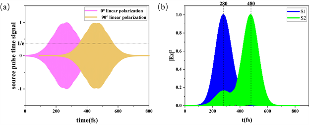
Figure 2. (a) Light source time pulse signal; (b) Time monitor results at positions S1 and S2

图2. (a) 光源时间脉冲信号;(b) S1和S2位置处的时间监视器结果

为了更清楚地观察到表面等离激元的转换过程,通过瞬时电场监视器观察SPP在不同时刻的激发路径,如图3所示,图3(a) T = 270 fs时表面等离激元SPP激发效果与(i)部分相对应,激发出的SPP在红点和黑点方向被检测到,我们发现激发的表面等离激元优先向X方向激发;图3(b) T = 365 fs时表面等离激元激发效果与(ii)部分对应,在黑点、白点、红点、紫点、四个方向都检测到SPP的存在,此时没有SPP定向激发的效果;图3(c) T = 500 fs时表面等离激元激发效果与(iii)部分对应,激发出的SPP在白点和紫点方向被检测到,SPP优先向Y方向激发。进一步证明了在整个转化过程中,表面等离激元的优先发射方向发生了超快时空切换。缺点是该结构只能控制SPP向X或Y方向激发,仅两个方向的选择性严重限制了SPP光路的发展。

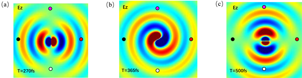
Figure 3. (a)~(c) Images of instantaneous near-field distributions of SPP directional couplers at different moments of time

图3. (a)~(c) 不同时刻SPP定向耦合器的瞬时近场分布图像

3.2. 双光束入射激发复合十字结构

图4(a)表示为复合凹槽结构时空操控fs-PSP定向激发的原理图,图4(b)为该结构的平面图,纳米结构尺寸L1 = 460 nm、L2 = 400 nm、d = 410 nm、w = 40 nm,目前,该结构已被实验验证了在空间中可以实现表面等离激元的定向激发 [21] ,通过控制入射光偏振来控制SPP的优先发射方向;同时该结构对圆偏振光也具备敏感性,结合时空控制方案,通过控制两束入射光的瞬时偏振态来实现fs-PSP定向激发。该结构定向激发表面等离激元的原理是:y方向的狭缝对将SPP发射到+x方向,x方向的狭缝对将SPP发射到+y方向。因此在不同偏振条件下,两个狭缝对产生的SPP干涉,可以激发出不同方向的等离激元。由于SPP在一个方向相长干涉,在另一个方向相消干涉,因此可以实现表面等离激元的定向发射,在−45˚~135˚范围内通过改变入射激发源的光学参数,激发出可控的SPP场,从而实现表面等离激元定向操控。

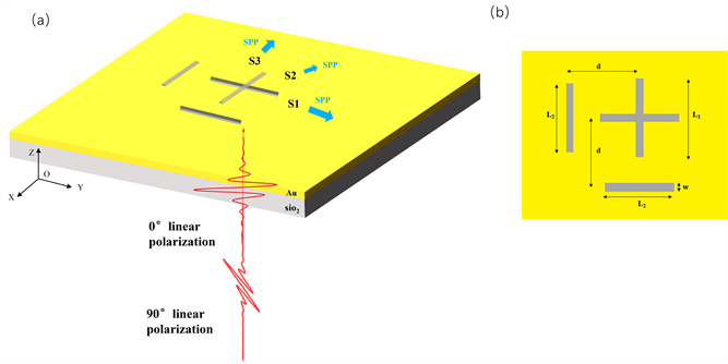
Figure 4. (a) Schematic of a structure capable of ultrafast spatio-temporal control; (b) Schematic of plane dimensions

图4. (a) 能实现超快时空调控的结构示意图;(b) 平面尺寸示意图

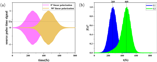
Figure 5. (a) Pulse time signals superimposed on two light sources; (b) Time monitor results for positions S1 and S3

图5. (a) 两束光源叠加的脉冲时间信号;(b) S1和S3位置的时间监视器结果

使用0˚ (P)偏振和90˚ (S)偏振两束线偏振飞秒脉冲入射激发该结构,相对时间延时为200 fs,光源叠加效果如图5(a);S1和S3位置时间点监视器的结果如图5(b),整个演化过程经历多种情况,在260 fs之前,P偏振光的前半部分入射定向耦合器,此时与Y轴平行的两个凹槽发挥作用,产生的SPP相互干涉最终在S1位置处激发;在460 fs之后S偏振光的后边部分作用在结构中,此时与X轴平行的两个凹槽发挥作用,SPP在S3位置处激发;转化过程中间部分的入射光由P偏振光的后半部分和S偏振光的前半部分相互叠加而产生,该光束激发的SPP在S2位置向外传播,后续通过观察不同时刻的瞬时电场可证明这一观点;因此在整个转化过程中,表面等离激元的优先发射方向经历了S1-S2-S3的过程。

为了更直观地呈现SPP优先发射方向的瞬时变化,首先观察S1位置和S3位置的点监视器如图6(a),图6(b),在T = 250 fs时,只有0˚偏振光的前半部分作用到结构中,相当于P偏振光耦合进结构,SPP激发方向为+X;在500 fs时为90˚偏振光的后半部分进入发挥作用,相当于S偏振光耦合进结构,SPP激发方向为+Y;与空间层面的激发效果吻合,因此我们的模拟方案是合理的,具有可行性。

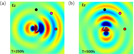
Figure 6. (a), (b) Instantaneous near-field distribution images for 250 fs and 500 fs SPP directional couplers

图6. (a),(b) 250 fs和500 fs SPP定向耦合器的瞬时近场分布图像

至此我们已经验证等离激元在该方案下可以实现优先激发方向的自主超快切换;如图7(a)~(c),分别为350 fs、365 fs、370 fs时刻的瞬时近场分布图,可以清晰的看出SPP优先激发方向从S1位置经历S2位置最终转移到S3位置,即:SPP的激发位置为“红点”–“粉点”–“黑点”;综上所述该复合十字结构能够在纳米飞秒尺度实现表面等离激元的超快时空调控。

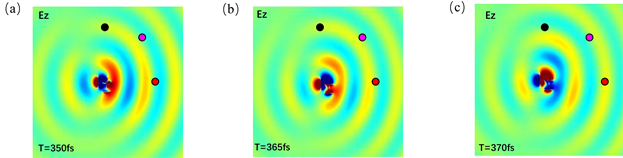
Figure 7. (a)~(c) Images of the instantaneous near-field distribution of the SPP directional coupler at three different moments, where S1 (red point) S2 (purple point), and S3 (black point) correspond to the positions in the structure picture

图7. (a)~(c) 三个不同时刻SPP定向耦合器的瞬时近场分布图像,其中S1 (红点)和S2 (紫点) S3 (黑点)与结构图中的位置相对应

4. 结论

总之,我们首先利用十字结构验证了实现表面等离激元的超快时空切换的方案,但发现其方向性受限,SPP激发缺乏自由度。为解决这一问题,我们探索并采用了一种经实验证明能够在空间中实现SPP定向激发的结构。通过同时叠加两束入射光应用到纳米定向耦合器,克服了SPP优先激发方向单一的难题,实现了飞秒时间尺度下的表面等离激元超快时空切换。与以往研究相比,我们为表面等离激元的发射方向提供了新的时空操控途径,其中主动控制SPP发射方向成为构建各类等离激元功能元件的关键一环。随着超快数据处理和传输的重要性不断凸显,对于实现SPP定向发射的超快时空控制变得尤为重要,这将有助于优化现有等离激元纳米电路组件中的超快信息处理系统,促进了等离激元器件的小型化集成化发展。未来,我们可以期待其在新型材料和结构设计、多功能性能器件、光通信、传感器、光学成像以及超快信息处理与计算等领域展现出更广泛的应用和进展。

致谢

感谢超快与极紫外光学重点实验室,林景全老师的辛勤耕耘和谆谆教导让我受益匪浅,借此论文写作之际,对其表示我最忠诚和崇高的感谢和敬意。感谢季博宇教授。从论文的选题、结构、成文、到反复的修改完善都倾注了老师大量的心血和精力,并提出很多宝贵的意见和建议,季老师优秀的科研思维,严谨的治学态度,以及真诚坦荡的处世之道,让我敬仰佩服。在此特别向季老师表示我最真挚的谢意和最美好的祝福。

另外,对本文写作中所参考和引用的国内外研究成果、著作、文献的作者表示最真挚的感谢。因为才疏学浅,以及掌握查询资料的不足,在论文的写作中难免有疏漏和不足,还希望各位专家学者老师提出批评指正,让我能够不断完善进步。

基金项目

等离激元聚焦透镜辅助的纳米粒子单点超短电子脉冲产生的研究;国家自然科学基金青年基金;62005022。

NOTES

*通讯作者。

参考文献

[1] Qin, Y., Ji, B., Song, X., et al. (2021) Ultrafast Spatiotemporal Control of Directional Launching of Surface Plasmon Polaritons in a Plasmonic Nano Coupler. Photonics Research, 9, 514-520.
https://doi.org/10.1364/PRJ.416633
[2] Guo, Q.R., Zhang, C. and Hu, X.H. (2016) A Spiral Plasmonic Lens with Directional Excitation of Surface Plasmons. Scientific Reports, 6, Article No. 32345.
https://doi.org/10.1038/srep32345
[3] Jin, J.J., Li, X., Guo, Y.H., et al. (2019) Polarization-Controlled Unidirectional Excitation of Surface Plasmon Polaritons Utilizing Catenary Apertures. Nanoscale, 11, 3952-3957.
[4] Sinev, I., Komissarenko, F., Bogdanov, A., et al. (2018) Switchable Directional Excitation Surface Plasmon Polaritons with Dielectric Nanoantennas. Journal of Physics: Conference Series, 1092, Article ID: 012140.
https://doi.org/10.1088/1742-6596/1092/1/012140
[5] Huang, T., Wang, J., Liu, W., et al. (2017) Spin-Controlled Directional Launching of Surface Plasmons under Oblique Illumination. Plasmonics, 12, 729-734.
https://doi.org/10.1007/s11468-016-0319-x
[6] Yao, S.Y., Guo, Z.Y., Sun, H.Q. and Huang, H.Y. (2018) Excitation of Direction-Tunable Surface Plasmon Polaritons by Using a Rectangular Array of Silver Nanodisks. Optics Express, 26, 20102-20110.
https://doi.org/10.1364/OE.26.020102
[7] Dabrowski, M., et al. (2016) Multiphoton Photoemission Microscopy of High-Order Plasmonic Resonances at the Ag/Vacuum and Ag/Si Interfaces of Epitaxial Silver Nanowires. ACS Photonics, 3, 1704-1713.
https://doi.org/10.1021/acsphotonics.6b00353
[8] Qin, Y., Ji, B., Song, X., et al. (2021) Efficient Plasmonic Functional Lens Constructed via a Nano-Dichroic Element. Journal of the Optical Society of America, B. Optical Physics, 38, C58-C62.
https://doi.org/10.1364/JOSAB.427300
[9] Lin, J., Mueller, J.P.B., Wang, Q., et al. (2013) Polarization-Controlled Tunable Directional Coupling of Surface Plasmon Polaritons. Science, 340, 331-33.
[10] Zhou, H., Qie, J., Dong, J., et al. (2018) Arbitrary Spin-Controlled Directional Coupling of Surface Plasmon Polaritons.
[11] Liu, Y., Palomba, S., Park, Y., et al. (2012) Compact Magnetic Antennas for Directional Excitation of Surface Plasmons. Nano Letters, 12, 4853-4858.
[12] Zhao, Z.L., Ji, B.Y., Wang, G.Q., et al. (2021) Symmetrical Double-Groove Structure as a Broadband Plasmonic Polarization Multiplexer. Optical Materials Express, 11, 2806-2816.
https://doi.org/10.1364/OME.428035
[13] Huang, F., Jiang, X., Yang, H., et al. (2016) Tunable Directional Coupling of Surface Plasmon Polaritons with Linearly Polarized Light. Applied Physics B, 122, Article No. 16.
https://doi.org/10.1007/s00340-015-6306-7
[14] Li, X., Tan, Q., Bai, B., et al. (2011) Experimental Demonstration of Tunable Directional Excitation of Surface Plasmon Polaritons with a Subwavelength Metallic Double Slit. Applied Physics Letters, 98, Article ID: 251109.
https://doi.org/10.1063/1.3602322
[15] Pisano, E., Garcia-Ortiz, C.E., Armenta-Monzon, F., et al. (2018) Efficient and Directional Excitation of Surface Plasmon Polaritons by Oblique Incidence on Metallic Ridges. Plasmonics, 13, 1935-1940.
https://doi.org/10.1007/s11468-018-0708-4
[16] Huang, X. and Brongersma, M.L. (2013) Compact Aperiodic Metallic Groove Arrays for Unidirectional Launching of Surface Plasmons. Nano Letters, 13, 5420-5424.
https://doi.org/10.1021/nl402982u
[17] Wu, Z. (2019) Polarization Controlled Couplings of Surface Plasmon with Asymmetrical Nanoslit Pairs. Current Applied Physics: The Official Journal of the Korean Physical Society, 19, 928-932.
https://doi.org/10.1016/j.cap.2019.04.008
[18] Tyagi, D., Chen, T.Y. and Huang, C.-B. (2020) Polarization—Enabled Steering of Surface Plasmons Using Crossed Reciprocal Nanoantennas. Laser & Photonics Review, 14, Article ID: 2000076.
https://doi.org/10.1002/lpor.202000076
[19] Gramotnev, D.K. and Bozhevolnyi, S.I. (2010) Plasmonics beyond the Diffraction Limit. Nature Photonics, 4, 83-91.
https://doi.org/10.1038/nphoton.2009.282
[20] Wang, Y.L., Ming, C.J., Zhang, Y.Q., et al. (2020) Spatiotemporal Manipulation on Focusing and Propagation of Surface Plasmon Polariton Pulses. Optics Express, 28, 33516-33527.
https://doi.org/10.1364/OE.405803
[21] Aeschlimann, M., Bauer, M., Bayer, D., et al. (2010) Spatiotemporal Control of Nanooptical Excitations. Proceedings of the National Academy of Sciences of the United States of America, 107, 5329-5333.
https://doi.org/10.1073/pnas.0913556107
[22] Johnson, B.P. and Christy, W.R. (1972) Optical Constants of the Noble Metals. Physical Review B, 6, 4370-4379.
https://doi.org/10.1103/PhysRevB.6.4370