1. 引言
二氧化锡(SnO2)作为一种良好的n型半导体材料,在显示器、光学玻璃、太阳能电池以及气敏元件方面有着重要的应用[1] -[3] 。但纯的SnO2材料导电性较差,所以通过向其掺杂其它元素,来获得集多种元素优点于一身的复合材料薄膜。目前对氧化铟锡(ITO)、氧化锌铝(AZO)、氧化锡锑(ATO)等氧化物透明导电薄膜的研究较为成熟。掺杂元素进入二氧化锡晶胞,形成替位原子,引起二氧化锡的带隙变化,有助于光生电子和空穴的分离,增强了薄膜的光透过性和导电性能[4] -[6] 。
本文选用与Sn4+半径相近的Nb5+进行掺杂,采用溶胶-凝胶法以及旋涂技术制备出SnO2:Nb复合薄膜,并对其光学、电学性能进行了测试。目前,国内外对SnO2:Nb薄膜研究较少,2013年李明超等[7] 制备出晶粒分布均匀的SnO2:Sb透明导电薄膜,并对其表面形态进行了研究。2013年Brion Bob等[8] 制备出粒径为2~4 nm的SnO2薄膜,该薄膜光学性能良好,可用于太阳能电池等方面。2015年殷馨等[9] 制备出锑掺杂氧化锡纳米粉体,对不同工艺条件下制备出的粉体结构与形貌进行分析。掺杂元素Nb的氧化物颜色比Sb氧化物颜色浅,所以更有助于获得透光度高复合薄膜,使得本文研究具有一定的新颖性。
2. 实验部分
2.1. 主要试剂与仪器
本实验中应用到的主要实验试剂见表1,实验过程中使用的主要仪器见表2。
2.2. 实验方法
称取一定量的氯化亚锡置于烧杯中,加入适量的无水乙醇,在80℃的恒温水浴下制得SnO2溶胶,分别向其中加入物质的量分数为5%、6%、8%、10%的Nb溶胶,将混合后的溶胶磁力搅拌4 h,最终得到浅黄色的SnO2:Nb溶胶。保鲜膜密封后,放入真空干燥箱静置陈化24 h,得到浅黄色透明SnO2:Nb凝胶。
采用匀胶机,在低转速下将湿凝胶滴加在预处理后的玻璃基片上,高转速下得到湿的凝胶膜,将膜
表1. 实验主要试剂
表2. 实验主要仪器
片放入真空干燥箱,烘干30 min,放入马弗炉中分别以200℃、300℃、400℃、500℃煅烧2 h,制得SnO2:Nb复合薄膜。
2.3. 样品表征
采用日本SmartLab智能X射线衍射仪分析样品结构,辐射源为Cu靶,工作条件为40 Kv,30 mA;日本JSM-6701F型扫描电子显微镜观察复合薄膜的表面形貌;英国VG公司的ESCALAB-250型X射线光谱仪对薄膜样品的掺杂元素含量、掺杂元素价态进行测定。
采用日本UV-2600紫外–可见分光光度计测定薄膜的紫外光吸收率,其光波范围是200~900 nm。RTS-9型双电测四探针测试仪测定薄膜的电阻。
3. 结果与讨论
3.1. XRD分析
图1是在不同热处理温度下SnO2薄膜样品的XRD谱图。从图中可以看出:200℃煅烧后,无特征峰出现,样品成无定型态。煅烧温度升高后(110)、(101)、(200)、(211)四个晶面出现明显的衍射峰,且强度越来越大。400℃煅烧后,(110)、(101)两晶面的衍射峰较宽,这种衍射峰宽化现象是由于晶体颗粒界面上的原子排列较为无序,存在着大量的氧空位和晶格缺陷。提高温度至500℃,得到了锋型尖锐,峰值较高的SnO2薄膜。衍射图谱与SnO2的标准卡片(PDF#41-1445)的主要谱线基本一致,表明生成了四方金红石型SnO2多晶结构薄膜。由此可见,煅烧温度越高,越有利于晶粒的生长。
图2是热处理温度为500℃,Nb5+掺杂量分别为0%、5%、6%、8%、10%的SnO2:Nb薄膜的XRD图谱。整体来看,图中衍射峰较为尖锐,晶化程度较高,结晶度好。与未掺杂的SnO2对比,谱图中没有新的衍射峰,说明无新相产生,Sn4+,Nb5+的离子半径分别为0.071 nm,0.064 nm,Nb5+以替代原子的形式进入SnO2晶胞。峰值整体略向低角度偏移,随着Nb5+掺杂量的增加,主峰值有所升高,Nb5+取代Sn4+

Figure 1. XRD patterns of SnO2 thin films calcined at different temperature
图1. 不同温度煅烧下SnO2薄膜的XRD图谱

Figure 2. XRD patterns of SnO2:Nb composite films
图2. SnO2:Nb复合薄膜的XRD图谱
的位置使得晶胞体积减小,晶格密度增大,掺杂量超过8%后,过多的Nb5+使得SnO2内部缺陷增多,晶格发生畸变。
3.2. SEM分析
图3为SnO2:Nb (Nb5+掺杂量为8%)复合薄膜的SEM图。在放大5万倍的情况下,薄膜表面较为平整,无明显的裂痕,有球状颗粒生成。左图为热处理温度为300℃的薄膜表面形貌图,可以看出生成的颗粒粒径分布不均匀,有团聚现象,温度升高到500℃(右图),薄膜表面颗粒分布的更加均匀,粒径较小,更为规整,约为10 nm左右。通过XRD和SEM图谱的综合分析,烧结温度在500℃较为合适。
3.3. XPS分析
图4为Nb掺杂量为8%的SnO2:Nb薄膜的X射线光电子谱图,从图中可以看到530.1 eV处是O1s的特征峰,486.3 eV处是Sn3d的特征峰,206.78 eV处是Nb3d的特征峰。实验数据显示Nb的掺杂量为6.85%,相较于理论值也有明显的损失,在实验过程中,pH值对铌溶胶的形成有很大的影响,pH值接近中性时铌溶胶容易以沉淀的形式析出,当Nb的掺杂量过大时,溶液中也有沉淀析出导致原料损失。

Figure 3. SEM photographs of SnO2:Nb composite films
图3. SnO2:Nb复合薄膜的SEM照片

Figure 4. X-ray photoelectron energy spectrum of SnO2:Nb composite films
图4. SnO2:Nb复合薄膜的X射线光电子能谱图
在图中280 eV处有杂质C1s的特征峰,主要是热处理时燃烧不充分导致的C残余和薄膜对含C有机物的吸附,可通过实验条件的改善来避免该特征峰的产生。
3.4. UV-Vis光谱分析
图5是Nb掺杂量分别为5%、6%、8%、10%的SnO2:Nb复合薄膜的UV-Vis谱图,根据图5的曲线可以看出掺杂过后的SnO2复合薄膜对波长400 nm以下的光有显著的吸收,其在可见光400~800 nm范围内几乎不吸收,表明SnO2复合薄膜对紫外光利用率较高。当Nb掺杂量为5%时,复合薄膜在紫外–可见光区基本无吸收,当掺杂量逐渐增加,薄膜对紫外光的吸收程度有了明显的增强,吸收曲线也随之产生了蓝移现象。这是由于Nb5+的掺杂使SnO2的费米能级向导带移动。掺杂Nb5+的量越多,SnO2的带隙就拓展的越宽,就能允许更高能量的光子通过,透过率增强。
3.5. 四探针电阻分析
将厚度约为0.05 mm的复合薄膜放入探针平均间距为1.00 mm的电阻仪中进行测试,测试结果取平均值记录到表3之中。薄膜的电导率随Nb5+掺杂量的增加而变化见图6。当掺杂量为5%时,薄膜的电导率较低,掺杂量为8%时,薄膜电导率有明显的升高。因为Nb5+代替Sn4+进入晶格中,占据了金属离子点阵,为了保持整体的电中性,需要进入更多数量的Nb5+,释放出更多的电子,这些电子的受到的束缚

Figure 5. UV-Vis Spectrum of SnO2:Nb composite films
图5. SnO2:Nb复合薄膜的UV-Vis谱图

Figure 6. Electric conductivity SnO2:Nb composite films with different content Nb-Doped
图6. 不同Nb掺杂量的SnO2:Nb复合薄膜的电导率
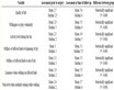
Table 3. Resistance measurement of SnO2:Nb composite films with different content Nb-Doped
表3. 不同Nb掺杂量SnO2:Nb复合薄膜的电阻测定
作用很小,可以在晶体中自由移动,提高了薄膜的导电性能。
从图6的曲线中可以看出,当Nb5+掺杂量从8%增加到10%时,电导率没有有明显的增加,这是由于Nb5+含量的增加,势必会导致SnO2晶格发生畸变,使得掺杂离子散射增强和内部缺陷增多,导致载流子的迁移率下降,复合薄膜的导电性能没有明显的提升。
4. 结论
采用溶胶–凝胶法以SnCl2·2H2O、NbCl5为原料,制备出SnO2:Nb透明导电薄膜,通过XRD、XPS两种测试手段,从定性和定量两个方面证明Nb5+以替代原子形式掺杂进SnO2晶胞中。
热处理温度为500℃,制得粒径为10 nm左右的SnO2:Nb复合薄膜,通过扫描电子显微镜观察到薄膜表面平整,颗粒分布均匀。通过结构测试分析得出:Nb掺杂量达到8%,晶型较好,结晶度高,掺杂超过8%晶格发生畸变。
由样品的紫外–可见光吸收光谱可以看出复合薄膜在紫外区有较强吸收,随着Nb5+的掺杂量增加薄膜对紫外光的吸收强度增强。薄膜的电导率随着Nb5+的掺杂量增加而增强。Nb5+掺杂量为8% SnO2:Nb复合薄膜具有较好的紫外吸收率及可见光透过率并且导电性能最好。
基金项目
吉林省教育厅“十二五”科学技术研究项目:吉教科合字[2013]第36号。